
Improved 4H-SiC UMOSFET with super-junction shield region*
2021-05-24 02:28PeiShen沈培YingWang王穎XingJiLi李興冀JianQunYang楊劍群ChengHaoYu于成浩andFeiCao曹菲
Chinese Physics B 2021年5期
關鍵詞:王穎
Pei Shen(沈培), Ying Wang(王穎),?, Xing-Ji Li(李興冀),Jian-Qun Yang(楊劍群), Cheng-Hao Yu(于成浩), and Fei Cao(曹菲)
1Key Laboratory of RF Circuits and Systems,Ministry of Education,Hangzhou Dianzi University,Hangzhou 310018,China
2National Key Laboratory of Materials Behavior and Evaluation Technology in Space Environment,Harbin Institute of Technology,Harbin 150080,China
Keywords: breakdown voltage, specific on-resistance, silicon carbide, switching energy loss, super-junction(SJ),trench gate MOSFET
1. Introduction
The advantages of silicon carbide (SiC) include a good wide bandgap performance, high electron saturation drift velocity, and high thermal conductivity.[1]The SiC is therefore very suitable for the development of the next-generation power electronic components that possess a high conversion efficiency,high voltage capability and low conduction loss. Furthermore, through simulation studies, Yu and Sheng[2]have shown the possibility that a SiC device can perform beyond its unipolar theoretical limit.
A SiC power trench gate MOSFET is a good candidate for serving as power switching in order to increase conversion efficiency. However, the UMOSFET does have a critical issue that it can generate a large E-field in the corner of the trench bottom, which affects the reliability of the device. To overcome this, some shielding methods and structures have been improved.[3–5]The most representative approach is to introduce the p+shielded region under the gate trench (conventional-UMOS).[6–9]However, the JFET region is formed between the p+shielded region and the p-base region, which increases the specific on-resistance. In order to achieve a better trade-off between specific on-resistance and avalanche voltage, a super-junction is a new structure, which improves the trade-off between specific on-resistance and avalanche voltage, and enables the low specific on-resistance in the industrial silicon power MOSFET.[10–12]Orouji et al.[13]studied the unique features that were exhibited by power in the 4H-SiC UMOSFET, where the n- and p-type columns in the drift region were incorporated in order to improve the breakdown voltage, on-resistance. In order to achieve lower on-resistance and better switching performance,Deng et al.[14]investigated a device structure that had a built-in floating component. In order to optimize the trade-off between on-resistance and short circuit ruggedness, He et al.[15]improved a 4H-SiC super-junction trench MOSFET by adding a grounded p+buried layer below the p-body,an oxide trench under the gate,and a p-region surrounding the oxide trench.
Moreover, the practical feasibility of fabricating superjunction structures has been discussed in some papers.[16–21]Kobayashi et al.[16]for example,reported that the SJ structure was formed on the drift layer by using multi-epitaxial growth seven times,gaining a thickness of 0.65μm each,and then the p-column was formed by implanting aluminum into the driftlayer and multi-epitaxial layers eight times in total. Furthermore, Kosugi et al.[17]developed a novel trench-filling epitaxial growth method as a promising alternative and Harada et al.[18]presented the first demonstration of the dynamic characteristics for a SiC superjunction MOSFET that was realized by the multi-epitaxial growth method.
This article investigates an improved 4H-SiC UMOSFET that has alternate p-type and n-type conductive pillars under the gate. The simulations indicate that the modified structure exhibits a good dynamic performance and improves the VBRand Ron,sp. The figure of merit of the conventional-UMOS is 563 MW/cm2, while the FOM of the modified-UMOS is 1008 MW/cm2. The VBRof the Gauss-doped structure is improved to 10.4%compared with that of the uniformdoped structure. The Gauss-doped and uniform-doped superjunction shield region gate–drain charges are the same.
2. Description of device structure and fabrica tion procedure
-
Figures 1(a)and 1(b)show the schematic cross section of a conventional-UMOS and a modified-UMOS,which are both used for reference. The detailed simulation parameters of the structure are listed in Table 1.
Figure 2 shows a feasible method of fabricating the modified-UMOS. An n-type epitaxial layer was grown on an n+substrate. The whole drift layer was about 10-μm thick with a doping concentration of 7.0×1015cm?3. The trench was formed by inductive coupled plasma reactive-ion etching (ICP-RIE) with SF6, O2, and HBr, using a Ni/Al2O3bilayer mask.[22,23]The n-pillars were formed by deposition[14]as shown in Fig. 2(a). The p-pillars, with a depth of 6 μm,were formed by a multi-epitaxial growth method[18]as shown in Fig.2(c).Finally,the p-body region,the light n-type current spreading layer,the n+source region,the p+source region,and the gate structure were implemented in a similar way to that adopted in the conventional-UMOS.
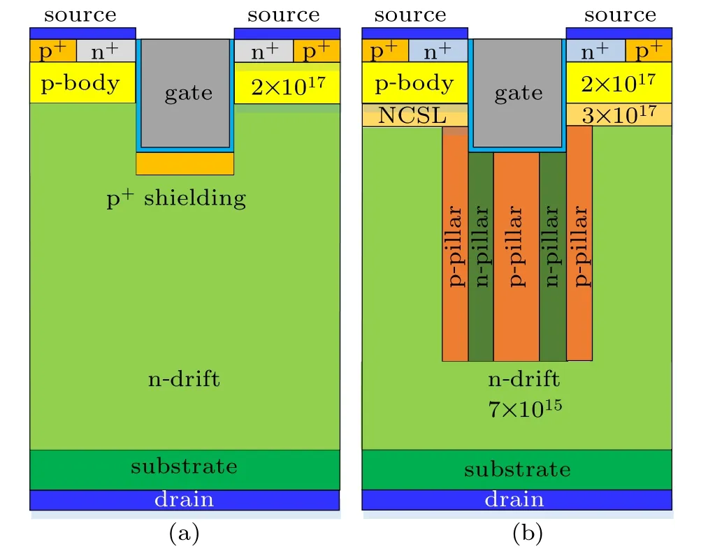
Fig.1. Structures of studied trench MOSFET:(a)conventional-UMOS,and(b)modified-UMOS.
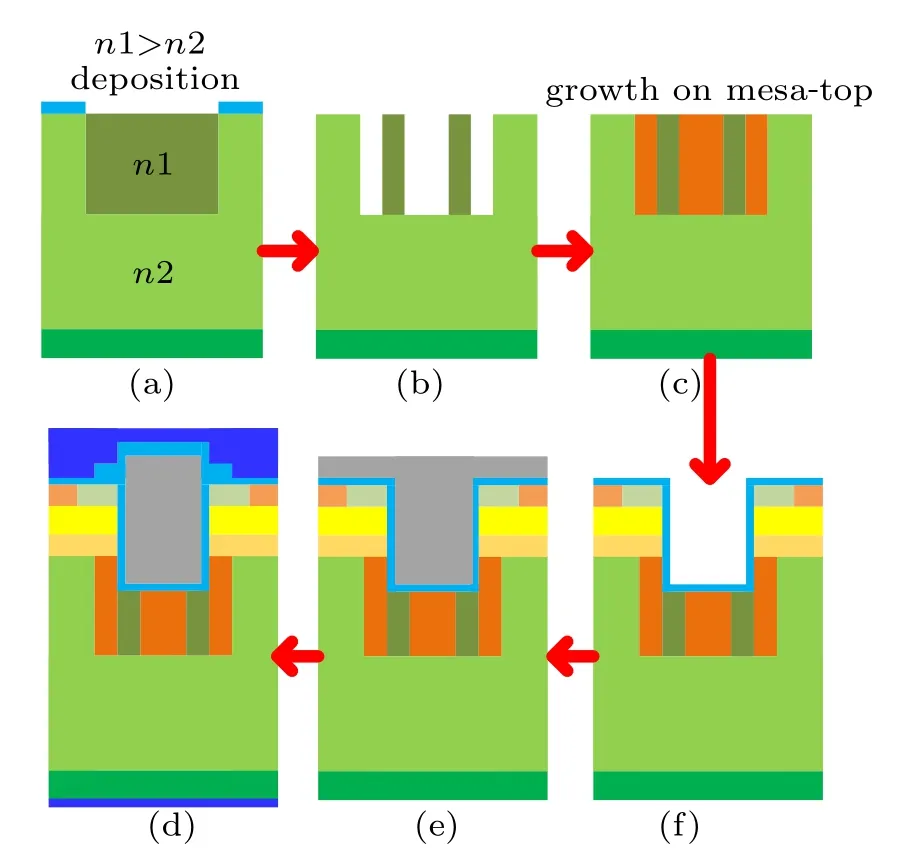
Fig.2. Key fabrication process for the modified-UMOS.
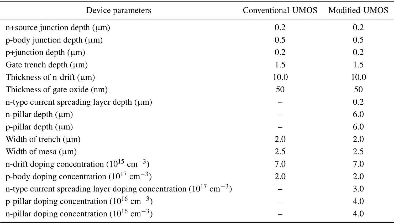
Table 1. Device parameters for simulations.
3. Results and discussion
In this work, the physical 4H-SiC MOSFET models, including the FLDMOB and ANALYTIC mobility models, are used. The FLDMOB is a parallel, E-field-dependent model,that requires the modeling of any type of velocity saturation effect;the ANALYTIC model is a concentration-temperaturedependent model;the Shockley–Read–Hall and AUGER models are composite models that are used to solve the electron/hole continuity equation, as well as the Poisson equation; IMPACT SELB is a Selberherr model and is recommended for most situations;and INCOMPLETE is an ionization model.[24]
3.1. Static performance
The two structures’ typical output characteristic curves of Vgs= 8 V, Vgs= 12 V, Vgs= 16 V, and Vgs= 20 V are shown in Fig. 3. The Ron,spof the modified-UMOS and the conventional-UMOS are estimated as ~1.9 m?·cm2and~2.4 m?·cm2at Vgs=16 V and Vds=1 V,respectively. The n-type conductive pillars and a thin NCSL provide two paths,which suppress the depletion region. The smaller the depletion region, the wider the current path for the electrons is.Moreover, a thin light doping of the NCSL causes the electrons to spread in the horizontal direction earlier. In addition,n-pillars under the gate allow the current to flow in the vertical direction. Therefore, the modified structure reduces the Ron,sp. Comparing with the conventional-UMOS,the Ron,spof the modified structure decreases by 22.2%. In the modified-UMOS, the n-type conductive pillars under the gate increase the electron concentration of the channel region,while the depletion region is reduced in order to increase the current path in the modified structure as shown in Fig.4.
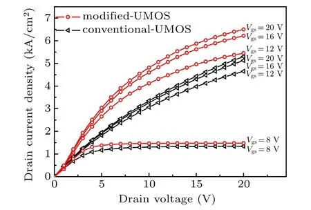
Fig.3. Typical output characteristic curves of two structures.
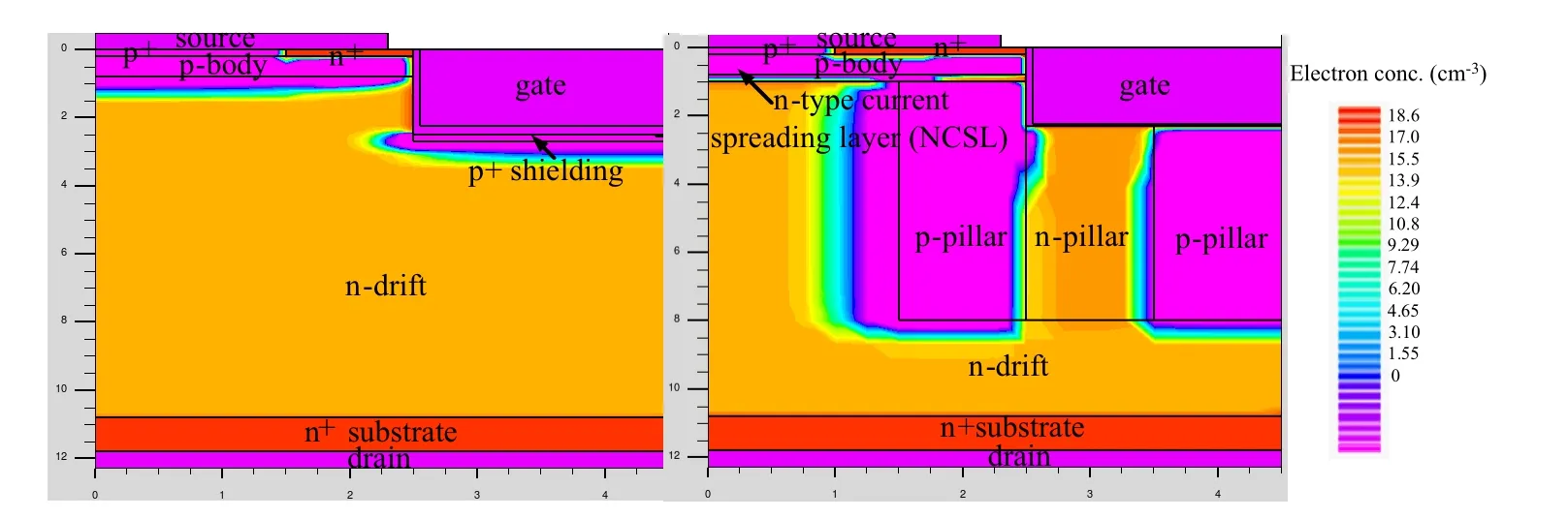
Fig.4. Distribution of electron concentration(Conc.) for(a)conventional-UMOS and(b)modified-UMOS.
The equation of the Ron,spcan be described as
where WDis the maximum depletion width and the μnis the electrons mobility.
Figure 5 shows reverse breakdown characteristic contours(at Vgs=0 V). The VBRof the two structures are calculated to be ~1167 V and ~1413 V respectively. The modified structure has a higher VBR,because the n-pillar and p-pillar at the bottom of the trench are configured to have a substantial charge balance in an SJ structure. When the doping density of the n-type conductive pillars is equal to the surface doping density of the p-type conductive pillars,the mutual depletion of the n-pillar and the p-pillar under the gate trench can achieve the charge balance of the SJ structure.
For the conventional-UMOS, the peak E-field (~3.3 MV/cm)occurs in the corner of the gate trench,whereas in the modified structure,the peak E-field(~2.6 MV/cm)occurs at the bottom of the p-pillars. The critical gate oxide E-field of a conventional UMOS is ~2.1 MV/cm, which is higher than the ~1.2 MV/cm belonging to the modified-UMOS as shown in Fig. 6. This difference occurs because the protruding p-pillar has an excellent shielding effect. During the simulation, the breakdown voltage for the modified-UMOS has an improvement of 21.1% compared with the the breakdown voltage of the conventional-UMOS.
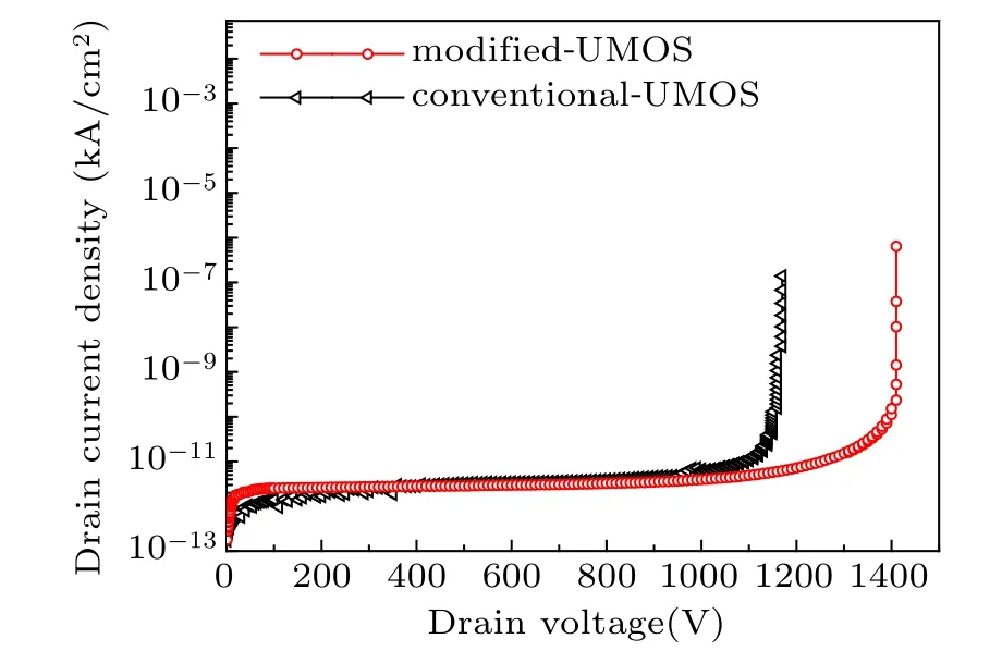
Fig.5. Reverse breakdown characteristic(at Vgs =0 V)curves of two structures.
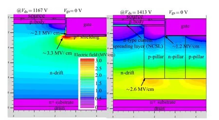
Fig.6. OFF-state critical E-field curves of(a)conventional-UMOS,(b)modified-UMOS.
3.2. Dynamic performance
Figure 7 shows the curves of the input capacitance Ciss[Ciss=Cgd(gate–drain capacitance) + Cgs(gate–source capacitance)] and the reverse transfer capacitance (Crss=Cgd).[25,26]The smaller Cgdhelps improve the switching characteristic.
The small ac signal works at 1 MHz to extract the capacitance,[27,28]and the capacitance cures of the modified-UMOS are not linear.[29,30]When Vds<Vt(at Vt= 75 V),the Crssis small because of the protruding p-pillar on the left,which shields Cgd. Thus,the capacitance at the bottom of the gate trench is mainly Cgs. When Vds>Vt, the p-pillar region will shrink,the shielding effect will be weakened and Crsswill slowly increase.
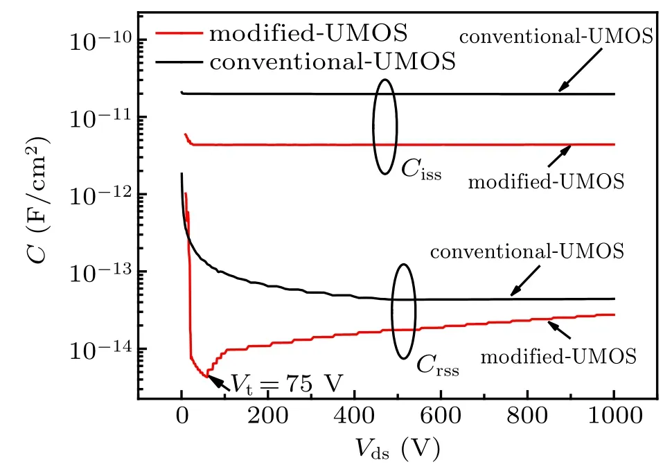
Fig.7. Small signal capacitances Ciss and Crss of two structures.
Figure 8 shows gate charge characteristic curves of the two structures.In the simulation,the test circuit is indicated as an inset in Fig.8. The FOM Ron,sp×Qgdis widely used.[31,32]Since the substantial charge balance of the SJ structure is achieved when the surface doping density in the p-type conductive pillar, the Qgdof the improved structure is a little smaller than that of the conventional-UMOS as can be seen in this figure. When the modified-UMOS is turned off,the twodimensional fast depletion of the n-type conductive pillar and p-type conductive pillar enables the charge carriers to be extracted quickly.The FOM Ron,sp×Qgdof the modified-UMOS shows an improvement of 43.3% in comparison with that of the conventional-UMOS. Detailed data are listed in Table 2.Using the double-pulse test(DPT),figure 9 shows the switching performance of the two structures. The area of the SiC MOSFET is set to be 0.09 cm2.For convenience,some parameters in the following simulation design are given as follows:a gate resistor is Rg=20 ?,the supply voltage is Vdd=400 V,the inductive load is LL=200 μH, and the stray inductance(LS)is assumed to be 10 mH in the power loop. The gate voltage is switched between 0 V and 20 V in order to turn-on and turn-off the device.
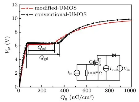
Fig. 8. Gate charge tests on the modified-UMOS (red line) and on conventional-UMOS(black line),with insert showing test circuit.
Figures 10(a) and 10(b) show the switching waveforms of the two structures with a test current of 20 A/cm2. As can be seen from Fig. 7, the low Crssin the modified-UMOS has a faster switching speed than that in the conventional-UMOS.Therefore,the conventional-UMOS needs a longer time period to arrive at a high Vdsand a high Idsas the switching characteristics are related to the charge and discharge of its Cissand the smaller Cisscan improve the switching characteristics.
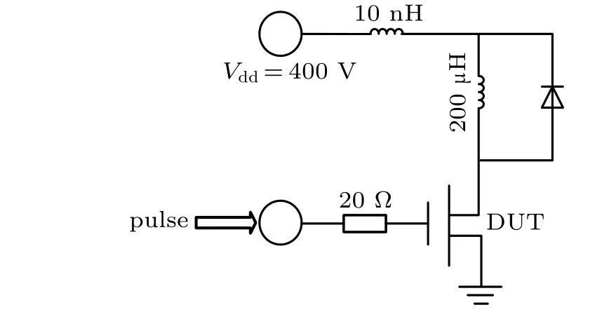
Fig.9. Double-pulse test circuit.

Fig. 10. Switching waveforms for (a) modified-UMOS and (b) conventional-UMOS,showing that improved structure is much faster than conventional-UMOS.
Figure 11 shows the switching energy losses for the conventional-UMOS and modified-UMOS. It can be discerned that in the modified structure, the losses during both turnon (Eon) and turn-off (Eoff) are reduced. For the modified-UMOS,the calculated value of Eonand Eoffare 33.5 mJ/cm2and 32.9 mJ/cm2,respectively,which correspondingly reduce 33.4% and 8.2% of the counterparts for the conventional-UMOS. The TOFFand TONof the two structures are listed in Table 2. The Eonand Eoffcan be expressed as
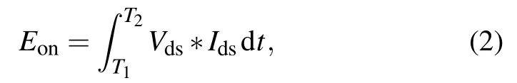
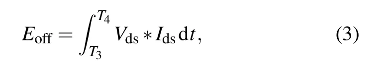
where T1is the time when Vgs(on) reaches 10% of its value,T2is the time when Vddarrives at 10% of its value, T3is the time when Vgs(on)rises to 90%of its value,and T4is the time when Idsis 2%of its value.
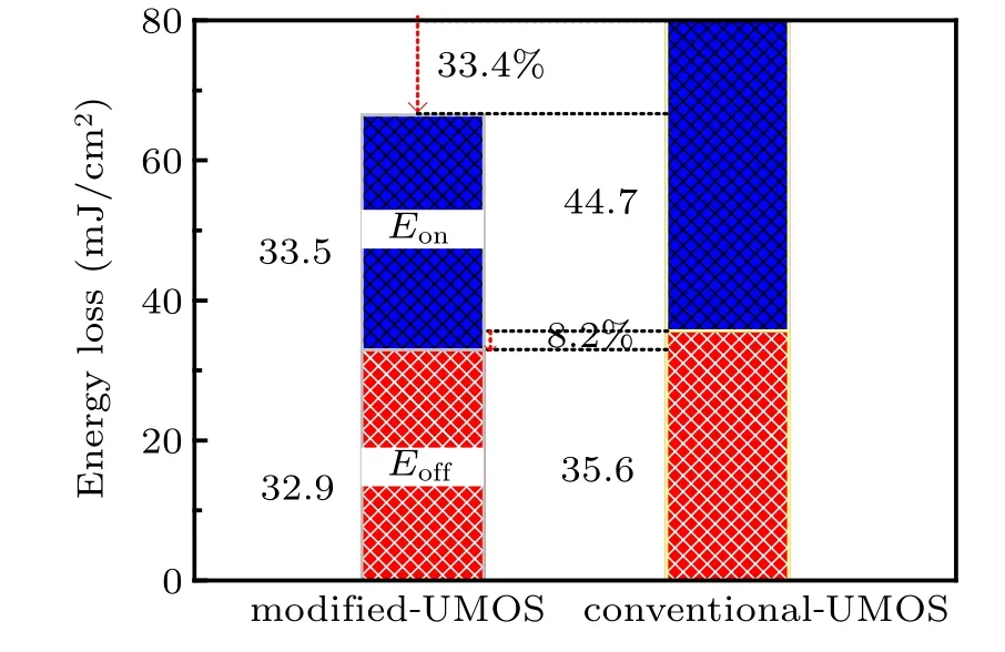
Fig.11. Switching energy losses of two structures.
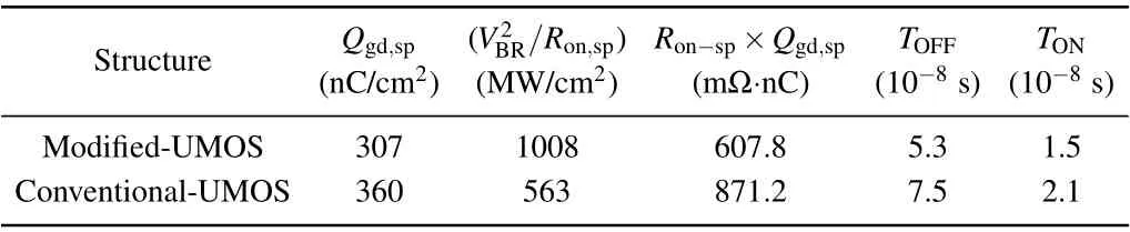
Table 2. Static performance and dynamic performance data.
3.3. Parameter optimization
Figure 12 shows FOM(V2BR/Ron,sp)as a function of Nrp,Nn, Nlp, and H in the modified-UMOS. The doping concentration(Nlp)of the protruding p-pillar,(Nrp)the p-pillar at the bottom of gate trench, (Nn), and the n-type conductive pillar,as well as the height (H) of pillars, have a great influence on the device performance. The p-type conductive pillars may have a doping concentration in a range from ~1×1016cm?3to ~1×1017cm?3. The doping concentration of the p-type and n-type pillars are denoted as Npand Nn,respectively,and the width of the p-type and n-type pillars are represented by Wpand Wn, respectively. The n-type pillar and p-type pillar at the bottom of the gate trench are configured to achieve a substantial charge balance in the SJ structure. This is achieved when the WncotNn=Wp·Np. If the conductive pillar is the one affected by the incomplete ionization,the current density is highly reduced, and the risk is that this leads to the total depletion of the p-type pillar, and consequentially, to no current flowing in the device.[33]The protruding p-pillar plays a critical role in shielding the high E-field of the trench bottom,therefore,the protruding p-pillar must have a high doping concentration in order to have the necessary efficacy to shield the high E-field. The Nncan be raised appropriately to reduce Ron,spand when increasing the doping concentrations of these pillars,Nrpand Nlpcan also be appropriately optimized to improve VBR.
The maximum figure of merit values appear at Nrp=Nn=4×1016cm?3, and Nlp=6×1016cm?3. Figure 13 shows the maximum figure of merit values of the modified-UMOS at H=6μm. When the value of H is greater than 6μm,the epitaxial layer is likely to be cut through. Therefore,H=6μm is selected for designing the n-pillars and p-pillars. Finally, the parameters in the above simulation and discussion are used.The figure of merit values of the two structures are calculated to be ~1.008 kV2/(m?· cm2) and ~0.563 kV2/(m?· cm2),respectively. The modified-UMOS is 79.0% higher than that of the conventional-UMOS.
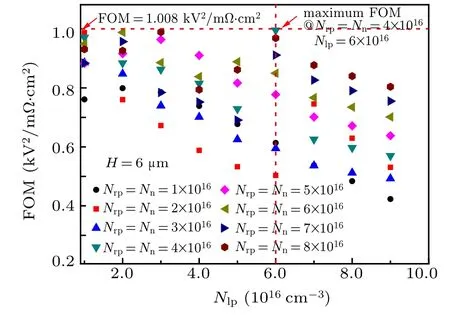
Fig.12. FOM(V2BR/Ron,sp)as a function of Nrp,Nn,and Nlp,and with pillar height H=6μm.
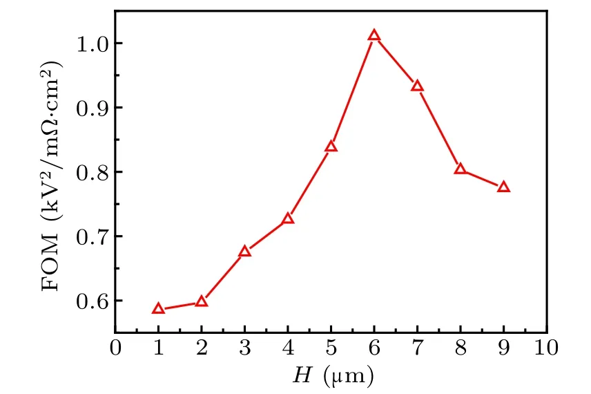
Fig.13. FOM versus column height of modified UMOS.
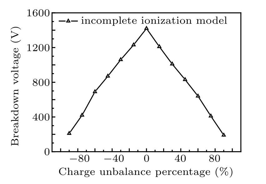
Fig.14. Simulated VBR versus unbalance ratio for device structure with the impact ionization model.
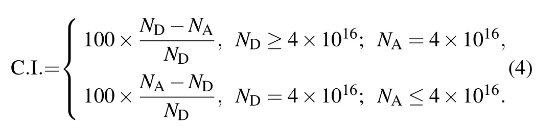
Figure 14 shows that the simulated VBRversus unbalance ratio for the device structure with the impact ionization models, where the unbalance ratio is defined as 100×abs(ND?NA)/max(NA, ND). For the balanced device, its charge imbalance (C.I.) is equal to 0% and is characterized by ND=NA=4×1016cm?3. The unbalance is indicated as a percentage and defined as
3.4. Gauss-doped super-junction shield region
The doping distribution in the super-junction shield region is shown in Fig. 15(a), in which the doping concentration in uniform-doped super-junction shield region is 4×1016cm?3, the doping concentration in Gauss-doped super-junction shield region is 1.0×1017cm?3, the doping concentration reduces 5.9×1015cm?3. Figure 15(b) shows the OFF-state characteristic curve of the Gauss-doped and uniform-doped region. The VBRof the Gauss-doped is improved to 10.4%compared with that of the uniform-doped region.
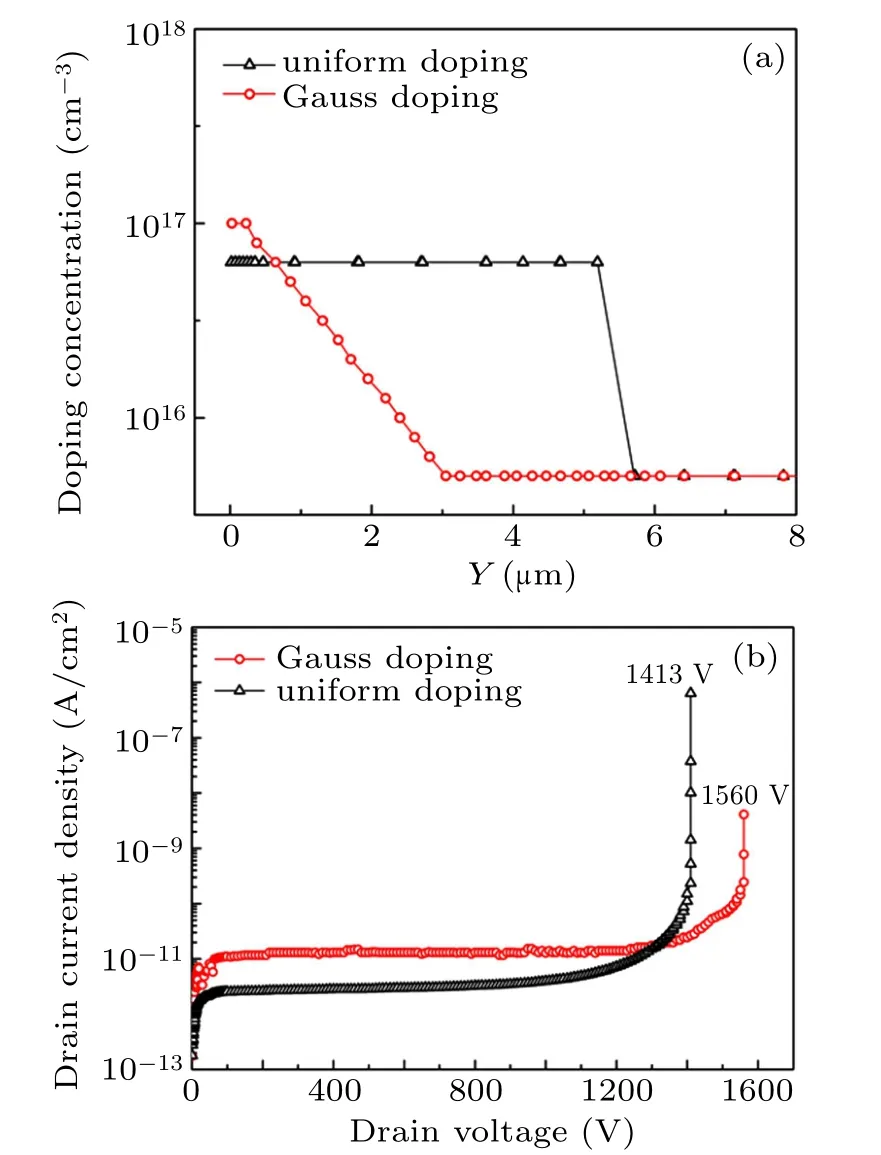
Fig. 15. (a) Variation of the doping concentration at super-junction of two structures with Y axis and (b) variation of drain current density with drain voltage in Gauss-doped region and uniform-doped region.
To compare the gate charges of the Gauss-doped and uniform-doped super-junction shield region, the gate charges of the two are simulated on condition that the total charge quantity of super-junction is the same, and the other parameters of the device are also the same. The time-varying curve of Qgand Vgsof the super-junction shield region are shown in Fig. 16. According to the calculation, the Qgdof uniformdoped super-junction shield region and Gauss-doped superjunction shield region are 307 nC/cm2and 327 nC/cm2. It can be seen that under the condition of the same total charge quantity of super-junction, gate-drain charge quantity in Gaussdoped and uniform-doped super-junction shield region are the same.
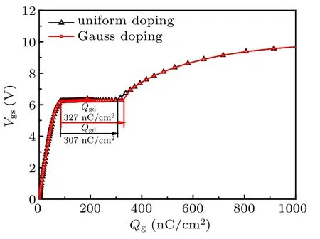
Fig.16. Simulation curve of gate charge characteristics of Gauss-doped and uniform-doped super-junction shield region.
4. Conclusions
In this paper, an improved 4H-SiC UMOSFET with alternate n-pillars and p-pillars under the trench is investigated.The Ron,spof the modified structure reduces 22.2%compared with that of the conventional-UMOS. Moreover, the critical gate oxide E-field of the conventional-UMOS is higher than that of the modified-UMOS.The results in the breakdown voltage is improved by 21.1%in comparison with the results of the conventional-UMOS, thus avoiding a premature breakdown of the trench gate oxide. Furthermore, the modified structure shows excellent dynamic characteristics and reduces the switching energy loss. The calculated values of Eonand Eofffor the modified-UMOS are 33.5 mJ/cm2and 32.9 mJ/cm2,respectively,which show a decrease of 33.4%and 8.2%respectively,in comparison with the results of conventional-UMOS.The modified-UMOS structure shows a significant improvement over the conventional-UMOS. In addition, the Gaussdoped super-junction shield region can increase the VBRof the device without degradation of dynamic performance. For device stability as well as switching speed considerations,we believe that the modified structure is more attractive and shows more promising for high power applications.
猜你喜歡
大觀(2022年9期)2022-12-06
Chinese Physics B(2022年7期)2022-08-01
農業災害研究(2022年1期)2022-05-07
青年文學家(2022年5期)2022-03-25
——中國傳統音樂學會第21屆年會綜述
人民音樂(2020年9期)2020-12-02
初中生世界·七年級(2019年8期)2019-08-29
文化交流(2019年12期)2019-01-09
東方教育(2018年3期)2018-03-30
東南大學學報(醫學版)(2015年2期)2015-03-22

- Chinese Physics B的其它文章
- Corrosion behavior of high-level waste container materials Ti and Ti–Pd alloy under long-term gamma irradiation in Beishan groundwater*
- Degradation of β-Ga2O3 Schottky barrier diode under swift heavy ion irradiation*
- Influence of temperature and alloying elements on the threshold displacement energies in concentrated Ni–Fe–Cr alloys*
- Cathodic shift of onset potential on TiO2 nanorod arrays with significantly enhanced visible light photoactivity via nitrogen/cobalt co-implantation*
- Review on ionization and quenching mechanisms of Trichel pulse*
- Thermally induced band hybridization in bilayer-bilayer MoS2/WS2 heterostructure?