
The low temperature growth of stable p-type ZnO films in HiPIMS
2021-09-10 09:26QianLI李倩MinjuYING英敏菊ZhongweiLIU劉忠偉LizhenYANG楊麗珍andQiangCHEN陳強
Plasma Science and Technology 2021年9期
Qian LI (李倩),Minju YING (英敏菊),Zhongwei LIU (劉忠偉),Lizhen YANG (楊麗珍) and Qiang CHEN (陳強)
1 Lab of Plasma Physics and Materials,Beijing Institute of Graphic Communication,Beijing 102600,People’s Republic of China
2 Key Laboratory of Beam Technology of Ministry of Education,College of Nuclear Science and Technology,Beijing Normal University,Beijing 100875,People’s Republic of China
Abstract In this study,the influence of substrate temperature on properties of Al-N co-doped p-type ZnO films is explored.Benefitting from the high ionization rate in high-power impulsed magnetron sputtering,the concentration of ionized nitrogen N+and ionized zinc Zn+were increased,which promoted the formation of ZnO films and lowered the necessary substrate temperature.After optimization,a co-doped p-type ZnO thin film with a resistivity lower than 0.35 Ω cm and a hole concentration higher than 5.34×1018 cm?3 is grown at 280 °C.X-ray diffraction results confirm that Al-N co-doping does not destruct the ZnO wurtzite structure.X-ray photoelectron spectroscopy demonstrates that the presence of Al promotes the formation of acceptor (No)defects in ZnO films,and ensures the role of Al in stabilizing p-type ZnO.
Keywords: HiPIMS,Al-N co-doped,ZnO film,substrate temperature,p-type conduction,N+/N2+
1.Introduction
As a II-VI semiconductor,ZnO is a promising film used in various industrial areas,such as transparent conductive electrodes[1],blue/UV light-emitting diodes(LEDs)[2],UV detectors[3]and solar cell devices[4],due to its high exciton binding energy(60 meV) and wide band gap (3.4 eV) [5].Based on these properties,ZnO films have wide ranging applications in photoelectric devices [6–9],where two of the key parameters are the high carrier concentration and the high mobility.The big challenge in p-n junction application based on ZnO film,however,is the instability of p-type conductivity.It is even concluded that based on conventional methods,it is difficult to form stable and low resistivity p-type N-doped ZnO,because of the formation of donor defects (possibly oxygen vacancies (Vo) and zinc interstitial(Zni)during the growth process),the small solubility of the acceptor of the N dopant in the ZnO body and subsequently transferring to(N2)o,and other issues.It then seems impossible to construct an efficient and stable N doped homogeneous ZnO p-n junction device [10].
Several techniques in film deposition such as molecular beam epitaxy (MBE) [11],pulsed laser deposition (PLD)[12],metal-organic chemical vapor deposition (MOCVD)[13]and magnetron sputtering (MS)[14]have been explored to prepare p-type ZnO film.Among them,the MS technique,owing to the advantages of easy control,good repeatability and high producibility,is considered to be one of the most promising methods for p-type ZnO film growth.
Regarding MS,the films prepared by high-power impulsed magnetron sputtering (HiPIMS) have always exhibited superior properties for both mechanical and structural properties because of the high ionization rate and the high reactive activity of sputtered species[15–18].Even it has been adopted to deposit ZnO film with a high carrier concentration [19],however,the stability of N-doped ZnO in p-type conductivity film is still under expectation [20].
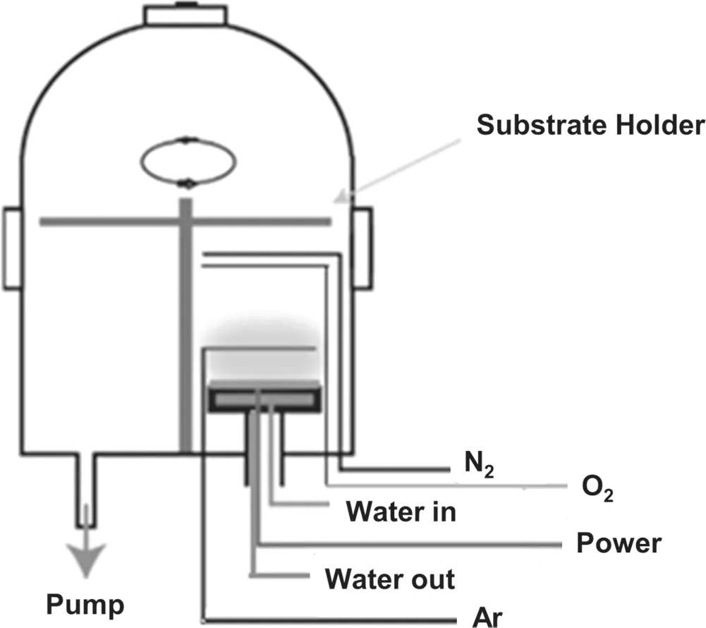
Figure 1.The schematic of the experimental setup.
As is known,N is the most proper dopant for p-type ZnO owing to being the same size as the O atom and the lowest ionization energy in V-group dopants [21].Although directly doping nitrogen with a NH3dopant is reported in the successful growth of p-type ZnO films[22],the use of N2as a dopant is still a challenge due to the poor repeatability and the poor stability of the prepared films[23].The use of co-doping,such as Al-N codoping,on the other hand,can significantly improve the deficiencies in N2as a dopant.The formation of the Al-N bond in doped ZnO greatly promotes the content of the doping Noacceptors,and its stability[24].But the high process temperature is unfavorable,and the reaction between Al and N,Al and O,as well as ZnAlO,i.e.the role of Al co-doping in the stability of p-type ZnO,has not been proved yet.
In this paper,Al-N co-doped ZnO films are prepared by HiPIMS where N2is introduced as a reactive gas,Zn and Al were co-sputtered from the one target.The influences of substrate temperature on the conductivity type,the optical and the electrical properties of ZnO films are studied.X-ray diffraction (XRD),an atomic force microscope (AFM),x-ray photoelectron spectroscopy (XPS),and Hall effect measurements are used to analyze the structure,the morphology and properties of as-prepared ZnO films.The purpose is to achieve a low temperature growth of p-type ZnO,to explore the possibility of using HiPIMS to prepare a stable p-type ZnO,and to affirm the role of Al in Al-N co-doped ZnO films.
2.Experiments
The home-made HiPIMS setup is shown in figure 1,which consists of a bell jar chamber with a base pressure of 1.2×10?3Pa.The oxygen and doping gases N2were separately introduced into the chamber and mixed with the argon working gas,which both were in the purity of 99.999%.An AlxZn1?xalloy (x=0.03) target was mounted on the cooled magnetron assembly.The target diameter is 100 mm,and the distance from the target to the substrate was 6 cm.Before moving the shield,the target was pre-sputtered for 3 min in order to remove the pollutants from the target surface.The Al-N co-doped ZnO films were grown on a glass substrate.The typical experimental parameters are listed in table 1.
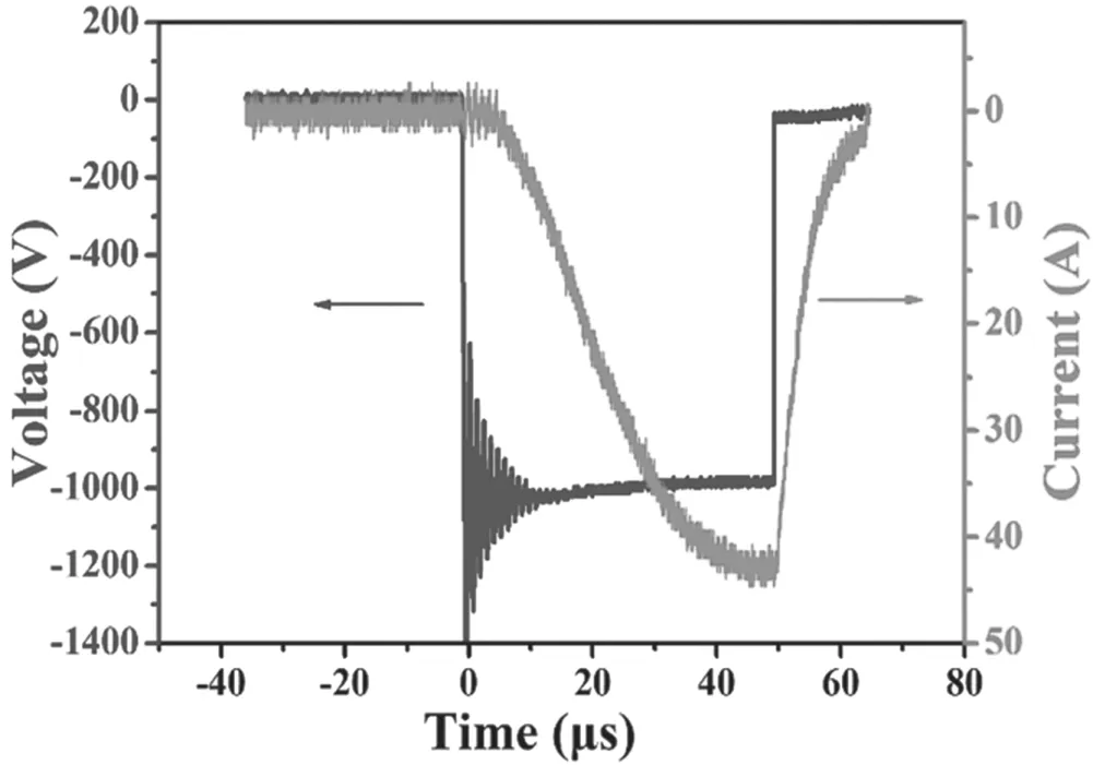
Figure 2.The waveforms of target voltage and discharge current in HiPIMS.
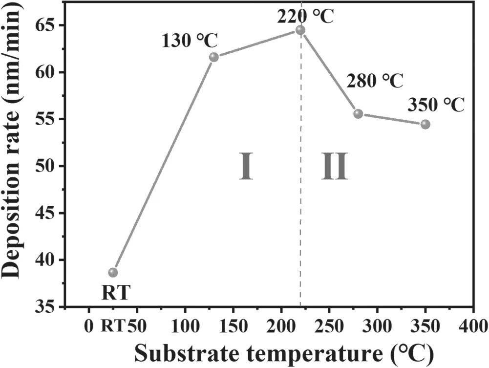
Figure 3.The deposition rate of ZnO films at various substrate temperatures.
The structural components of the films were analyzed by a XRD (Rigaku) spectroscope with a Cu-Kα source(0.15418 nm) and XPS (Thermo Scientific escalab 250 XI).The optical transmittance of the films was analyzed in the ultraviolet by Cary 5100 UV–vis spectrophotometer.The mobility,the resistivity,and the carrier concentration of asdeposited Al-N co-doped ZnO films were measured by ECOPIA HMS-3000 Hall effect measurement equipment.The conduction type of the ZnO films was determined by both Hall and Seebeck effect measurements.The surface morphology of the films was characterized by AFM (Veeco DI INNOVA)operated in tapping mode.During the sputtering process,the current and voltage characteristics were recorded by an oscilloscope(Tektronix DPO 4104).As seen in figure 2,the 1200 V square-wave voltage was applied to the target,and the currentwas increased slowly in the rising edge,but decreased dramatically in the falling edge after reaching to the peak current of 43 A,which indicated that the discharge was in the HiPIMS mode.

Table 1.The typical deposition parameters of Al-N co-doped ZnO films.
3.Results
3.1.Deposition rate
Considering the temperature effect in Al-N co-doped ZnO film growth,the deposition rate was firstly measured.Figure 3 shows the deposition rate versus the substrate temperature.It is noticed that the ZnO film grew in two modes: when the temperature was below 220 °C the deposition rate increased with increased temperature,from 38.64 nm min?1at room temperature to 64.49 nm min?1at 220°C.when the substrate temperature was over 220 °C,the deposition rate decreased with the growth temperature.At a temperature of 350°C,the growth rate was reduced to 54.44 nm min?1.The reason for the slight decrease of the deposition rate at high substrate temperature is the desorption of species from the substrate.As the substrate temperature is high,the kinetic energy of the adsorbed atoms on the substrate surface is increased,the condensing process between the adsorbed atoms is enhanced.However,if the substrate temperature is too high,the species desorption dominates.As a result,the deposition rate is reduced.
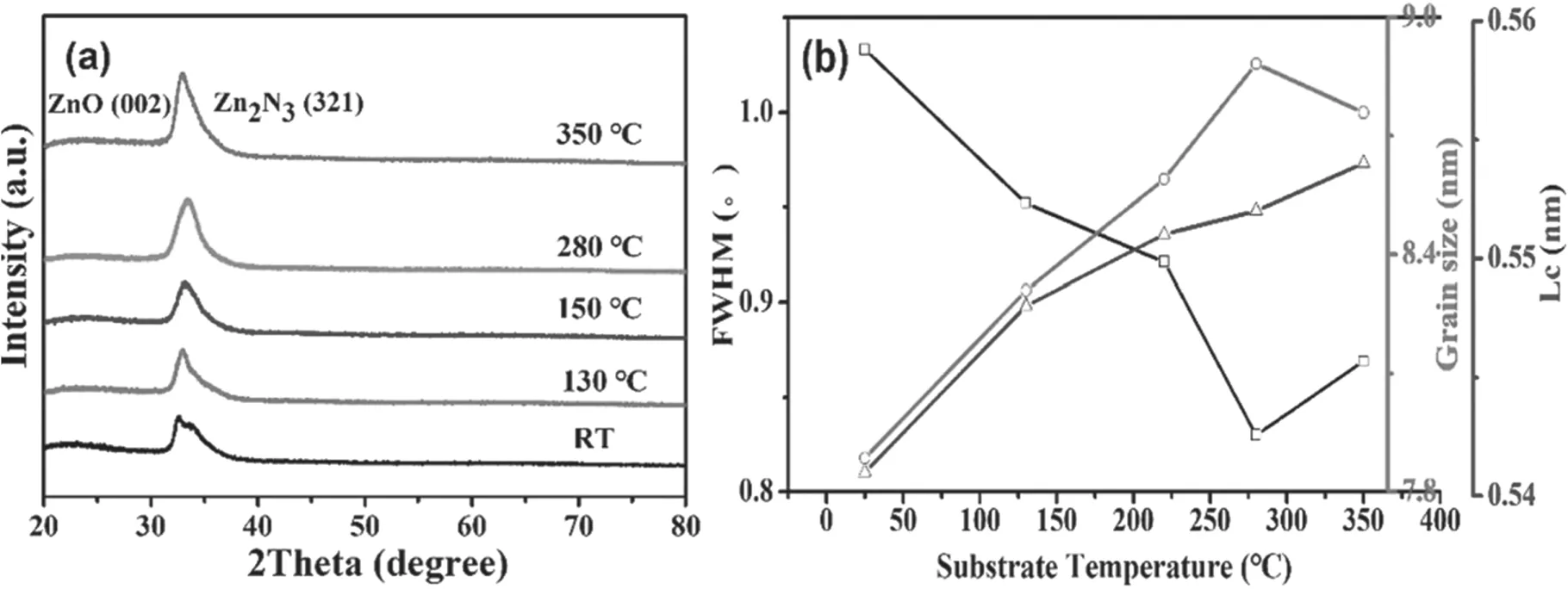
Figure 4.(a)The XRD patterns of as-deposited ZnO film versus the deposition temperature and(b)the influence of substrate temperature on ZnO crystalline.
3.2.X-ray diffraction (XRD)
Figure 4(a)shows XRD patterns of ZnO films deposited at the various substrate temperatures.One can see that all the ZnO films were preferentially a grown (002) facet,i.e.Al-N codoping did not destruct the ZnO wurtzite structure (JCPDS 36-1451).It is noted that with the increase of temperature the intensity of the (002) diffraction peak was gradually increased.Based on the reduced deposition rate at the high temperature shown in figure 3,the increasing intensity may be the fact that the diffusion of the atoms adsorbed on the substrate surface was increased,and the acceleration of the atom migration to a suitable nucleation site was improved.
In addition,the diffraction peak of zinc nitride (Zn2N3)(001) was significant.The existence of Zn2N3(321) caused the (002) peak to appear asymmetric as figure 4(a) shows.This indicates that N was combined with the excess Zn in the film,reducing the concentration of the Zn interstitial (Zni)which is the donor defect,thus reducing the self-compensating effect [25].
The grain sizes (L) and lattice constant (Lc) were calculated to further analyze the film microstructures.In figure 4(b),with the increase of substrate temperature from room temperature (RT) to 350 °C,the lattice constantLcof wurtzite structure ZnO was increasing gradually,which implies that N atom concentration in films was increasing because the ionic radius of O2?is smaller than that of N3?[26].
Figure 4(b) indicates that the crystallinity was improved along with increased substrate temperature.The grain sizes were enlarged at the beginning and then decreased along with the increased substrate temperature.The high temperature caused the adsorbed particles to migrate with enough kinetic energy,which made the nucleation sites on the surface distribute in uniformity.When the increased temperature was over 350 °C,the high kinetic energy led to the radical quick immigration,even desorption.The nucleation centers were disordered and unstable and,as a result,the grain size became smaller [27].
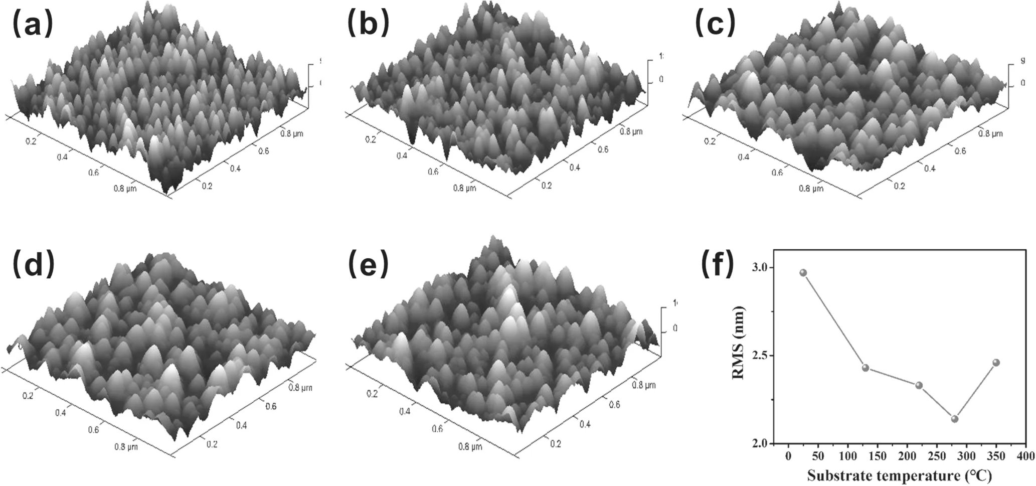
Figure 5.AFM 3D images of Al-N co-doped ZnO films with various substrate temperatures.((a) RT,(b) 130 °C,(c) 220 °C,(d) 280 °C,(e) 350 °C,(f) surface roughness).
3.3.Surface morphology
The surface morphology and roughness of ZnO films influenced by the deposition temperature were examined by AFM images.Figures 5(a)to(e)indicate that the domain sizes were increased when the temperature was raised from room temperature to 280 °C,but decreased with further increase at 350 °C.As seen,the crystallinity of the films was improved based on the particles being much more regular along with the temperature.This is consistent with the results determined from the XRD pattern in figure 3.
Figure 5(f) summarizes the surface roughness,which implies that the films were quite smooth,but the smoothness depended on the substrate temperature.When the substrate temperature was under 280 °C,owing to the preferential of crystal orientation,the root mean square(RMS)dropped with increasing temperature.However,when the temperature was over 280 °C,the more nucleation centers were formed,and the growth mode changed from layer-by-layer to mixture growth mode,and the surface then became a little bit rough.
3.4.Electrical characterization
Figure 6 shows the dependence of electrical resistivity,Hall mobility and carrier concentration of the Al-N co-doped ZnO thin films on the substrate temperature.It is noticed that when the substrate temperature was raised from room temperature to 280 °C,the electrical properties of ZnO films were improved remarkably: the resistivity decreased linearly from 1291 Ω cm at RT to 0.35 Ω cm at 220 °C,and slightly increased at 350 °C.The carrier concentrations were jumped from 1016to 1018Ω cm at 220°C,and dropped to 4.1×10¹⁸at 350 °C.It was more than two orders of magnitude larger than that prepared in only N2doped ZnO film,where the carrier concentrations of p-type N doped ZnO were in the range of 1014?1016cm?3[28].This indicates that the doped Al can effectively promote the concentration of (N)oor Zniacceptors as hole carriers in p-type ZnO.At 280°C the carrier concentration in Al-N co-doped ZnO was maximized at 5.34×1018cm?3.
Figure 6 exhibits that the change of carrier mobility in Al-N co-doped ZnO did not follow the trend of carrier concentration.From RT to 130 °C the mobility was sharply dropped,and then gradually increased to 3.41 cm2V?1at 280 °C,then falls a little bit again at 350 °C.The reason might be relevant to the crystallinity and the surface roughness of films.When the film was deposited at room temperature,the crystallinity was significantly improved,the immigration of holes was then blocked.With the increase of crystal domain and the decrease of amorphous domain,the mobility was increased until 280 °C.when the temperature was over 280 °C,the surface roughness was increased,scattering effect was increased,and the small domain resisted the hole movement.The adsorbed oxygen at the high temperature can capture holes,dropping the carrier concentration and mobility,resulting in the increasing electrical resistivity [29].Compared with previous studies [30–32],the mobility of films deposited at substrate temperature above 150 °C is acceptable.Up to now,the low mobility,and the small hole concentration remain as obstructions for applications of p-type ZnO in the field of optoelectronics.So,to remove the impurities introduced into the ZnO lattice through the doping process might be the better solution.
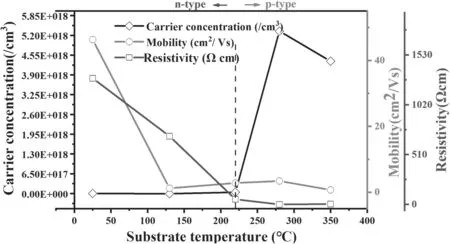
Figure 6.The relationship between resistivity,carrier concentration and mobility of Al-N co-doped ZnO films and the substrate temperature.
Notice in figure 6 that the films deposited in the range of RT to 130 °C show n-type conduction,while p-type conduction films are obtained in the range of 220 °C to 350°C based on Hall effect measurement,which were confirmed by Seebeck coefficient measurement.
Whether p-type ZnO films can be obtained by co-dopingⅢgroup elements with N strongly depends on the substrate temperature during the growth of the films.As it is known that N as an interstitial atom immigrated slowly at a low temperature,the intrinsic defects such as VZnand Oibecame the main factors determining the conductivity type of films[33],and the film exhibited n-type conduction when it was grown below 220°C.When the substrate temperature is low,the acceptor energy is low and it is difficult to diffuse to the appropriate lattice position,so only n-type ZnO thin films with low carrier concentration can be obtained.Meanwhile,at low temperatures there is not enough energy for Al and N atoms to replace Zn and O,respectively.With the increase of the substrate temperature,the number of activated nitrogen atoms increases,resulting in the increase of the hole concentration in the film.However,when the deposition temperature exceeds 220 °C,the number of active nitrogen atoms increases,and the N species form Nodefects as acceptors by high kinetic activation,resulting in the increase of hole concentration in the films.The conductivity type of the film changes to p-type,even though there are still inherent defects in the film,it cannot completely make up for the Nodefects.
3.5.Stability of p-type ZnO
The stability of p-type ZnO is the challenge in homogeneous ZnO p-n junction device application,because after one or two weeks of storage,the conductivity of the film will switch from p-type to n-type.The mechanism has been explored extensively.But our results demonstrate that the p-type conduction can be maintained for more than 6 months if HIPIMS was employed to deposit Al-N co-doped ZnO film.However,the carrier concentration in the p-type ZnO was continually decreased in the storage period for both samples prepared at 280 °C and 350 °C as figure 7 shows.
3.6.Optical study
Figure 8(a) shows the transmittance of Al-N co-doped ZnO films versus the deposition temperature.When the deposition temperature was over 220°C,the transmittances were similar,and in the visible range the transmittance was above 85%for all films.The large modulation observed in the curves is due to the multiple interference streaks of light reflected at the interface and at the surface between the co-doped ZnO films and the glass substrate [34].The interference implies the flatness of the film surface.Figure 8(b)indicates that the band gap was increased with the increased substrate temperature.A similar result was observed by Zhuet al[35].This may be due to the increase in the lattice constant and the decrease in the Coulomb interaction among atoms [36].
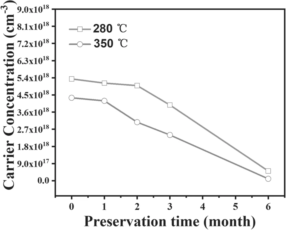
Figure 7.The variation of carrier concentration versus storage time.
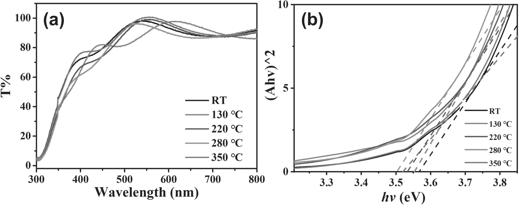
Figure 8.(a) The transmittances of Al-N co-doped ZnO films deposited at room temperature,130 °C,220 °C,280 °C,and 350 °C,respectively; (b) the calculated band gap from absorption versus photon energy.
Table 2.The process parameters in DCMS and HiPIMS for plasma diagnostics.
From the aforementioned results it can be concluded that the HiPIMS technique is an efficient tool to prepare Al-N codoped p-type ZnO films where N2was introduced as a reactive gas and Zn and Al were co-sputtered from the target.The conductivity type,mobility,and the carrier concentrations were suitable for the fabrication of a homogeneous ZnO p-n junction device.Therefore,the reason of stable Al-N codoped p-type ZnO films by HiPIMS shall be explored.
As stated,high ionization induced reactions can stabilize Nodefects in the crystal if N2is used as dopant,and there are two main defects in nitrogen doped ZnO:(1)N atoms replace O atoms in the lattice to form (N)odefects; (2) nitrogen molecules replace oxygen atoms in the lattice to form (N2)odefects,but only(N)oacceptors are stable in p-type ZnO film[37].Therefore,increasing concentration of(N)oacceptor and avoiding the formation of (N2)odonor in the films are essential for stable p-type ZnO growth.The broken N-N bond and the reaction induced by nitrogen ionic status in HiPIMS certainly benefit the (N)oformation and stability.
N ions in HiPIMS were diagnosed by optical emission spectrometry (OES) (Netherlands,Ava-Spec 2048×14-5-USB2),which also distinguished N+or N2+joining the induced reaction in Al-N doped film growth,as comparison N2gas discharge in direct current MS (DCMS) was diagnosed.The discharge parameters of DCMS and HiPIMS are listed in table 2,and the lines of 463 nm and 391.3 nm for N+and N2+were selected in the analysis,respectively.
Figure 9(a) shows the ratio of N+/N2+in DCMS.One can see that the ratio of N+/N2+is increased along with the applied power.When the applied power was 250 W,the ratio of N+/N2+was 0.192; while at 400 W,a maximum N+/N2+value of 0.272 was obtained.
In figure 9(b),on the other hand,when the DCMS was replaced by HiPIMS,the N+/N2+is always increasing with the increase of discharge voltage or power.Based on the data in figure 2,i.e.50 μs of pulse width,1200 V of voltage,43 A of the peak current,1% of duty ratio,the average power of HiPIMS can be calculated from equation (1):
when the peak power was about 16 kW and the average power was about 160 W,the ratio of N+/N2+was 0.277.In this case of the 160 W for same power in DCMS,the ratio of N+/N2+was only 0.118.When the peak power was about 25 kW and the average power was about 250 W,the ratio was 0.873.At the same power of 250 W in DCMS,the ratio of N+/N2+was as small as 0.192,i.e.the ratio of N+/N2+in HiPIMS was 5 times higher than that in DCMS condition in the same applied power.It completely confirms the high ionization in HiPIMS and reasonably explains the high (N)oconcentration in the deposited ZnO film.
Film structure analysis further gives evidence of the ionization induced reaction during Al-N co-doped ZnO growth.Figures 10(a),(b) and (d) show XPS analysis results of as-growth film deposited at 280°C.For undoped ZnO,the peak position of Zn2p3/2is located at 1021.3 eV,while it is located at 1024.3 eV for doped ZnO [38],there is a 3 eV right-shift.Figure 10(b)shows the core level of Al2p.There is only one peak at 74.5 eV,which is related to the Al-N bond.The peak shifted from 74.5 eV to 74.2 eV might indicate Al-2N bond cluster formation [39],which is correlated to the ionic induced reactions in HiPIMS [40].The Al-N bond formation benefits the stable (N)odefect in the crystal,and it is also responsible for the high carrier concentrations in ZnO films by increasing the content of (N)oacceptors in the defects.
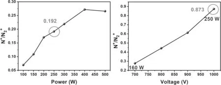
Figure 9.The ion ratio of N+/N2+ versus applied power in (a) DCMS and (b) HiPIMS.
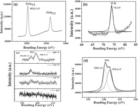
Figure 10.XPS of core levels (a) Zn2p3/2,(b) Al2p,(c) N1s,and (d) O1s in Al-N co-doped p-type ZnO thin films.
Figure 10(c)is the core level of N1s.It is found that when the substrate temperature was lower than 220°C,the intensity of the N1speak was very weak or not observed.When the temperature exceeded 220 °C,a significant peak value appeared around ~396 eV.In addition,a new peak at 398.5 eV appeared for 280oC deposited sample.The peak located at 396.05 eV corresponded to (N)odefects,while the other peak located at 398.5 eV was caused by the Al-N bonds[41].The (N)opeak at 404 eV for (N2)oappeared in the spectrum.It is inferred that N and Al presented in ZnO were mainly in the state of Al-N bonds,and the presence of Al indeed facilitates the incorporation of N.According to Yanet alreported[42],the intensity of N1speak was related to the concentrations of(N2)oand(N)oin ZnO films,no peak at 404 eV means that major doped N might replace the lattice O.
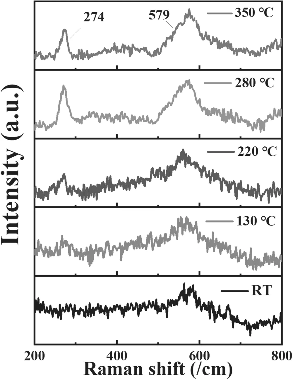
Figure 11.Raman spectrum of Al-N co-doped ZnO films deposited at various substrate temperatures.
Figure 10(d)shows a core level of O1sin Al-N co-doped ZnO film.It is noticed that O1speak was asymmetric,which was deconvoluted into two peaks at 530.1 eV and 531.6 eV,respectively.The peak at 530.1 eV was attributed to the formation of O2?[43],which was caused by oxygen molecules adsorbed on the surface or grain boundary,while the peak at 531.6 eV was related to interstitial oxygen (Oi) [44].Oiis a potential source of p-type ZnO conductivity,and possibly contributes to the mobility and the stability [45].
XPS measurement revealing N substitution O in the lattices is confirmed by Raman results as shown in figure 11.One can see that one significant peak was located at 274 cm?1,originating from lattice distortion or related to the defects of Zni-Nocaused by N incorporation [46].The other peak at 579 cm?1,called A1(LO)the phonon vibration mode,is generally related to Voand/or Zniand composite defects.It is found that the peaks at 274 cm?1and 579 cm?1increased with increased substrate temperature.When the substrate temperature was 280 °C,the peak intensity was the highest,indicating that the density of(N)odefects was increased.It is worth noting that the E2(high) mode did not appear in the spectrum.The possible reason is that internal defects and external dopants cause the destruction of translational symmetry [26].
4.Conclusions
In summary,the influence of deposition temperature on p-type Al-N co-doping ZnO films through the HiPIMS technique has been investigated.Our study exhibited that using HiPIMS could lead to a reduced substrate temperature and still realize p-type conductive film deposited at relative low temperature,which is conducive to promoting the application of p-type film on various fields.In addition,a suitable deposition temperature could even improve electrical properties,crystalline quality and the surface roughness of the films.Under optimal process parameters,a p-type ZnO film with the resistivity of 0.35 Ω cm,the mobility of 3.41 cm2V?1s?1,and the hole concentration of 5.34×1018cm?3could be grown at 280 °C,and maintaining in p-type conductivity over a half year,which makes it possible to fabricate the ZnO transparent p-n junction and the fundamental structure of these optoelectronics devices.
Furthermore,after analysis of the film structure,it was concluded that co-deposition of Al played a role in p-type Al-N co-doping ZnO stability,the formation Al-N bond promoted(N)odefect stability in the crystal,because the ionic induced reaction between N and Zn during reactive magnetron sputtering provided the formation of p-type N-doped ZnO film when N2was used as a dopant.Therefore,it is believed that HiPIMS is a promising tool to grow the stable p-type ZnO film.
Acknowledgments
The project was supported by National Natural Science Foundation of China (Nos.11875090,12075032,11775028,11875088,11974048),Beijing Municipal National Science Foundation (Nos.1192008,KZ202010015022) and BIGC(Nos.Ea201901,Ee202001).
猜你喜歡
Plasma Science and Technology(2022年8期)2022-09-14
三悅文摘·教育學刊(2021年52期)2021-04-27
黃河黃土黃種人(2018年10期)2018-12-17
美與時代·城市版(2018年6期)2018-09-14
藍盾(2016年7期)2016-07-29
藝術評論(2016年5期)2016-05-14
黃河黃土黃種人(2016年4期)2016-05-04
戲劇之家(2016年1期)2016-02-25
故事會(2015年19期)2015-05-14
微型小說選刊(2014年7期)2014-11-15
 Plasma Science and Technology2021年9期
- Plasma Science and Technology的其它文章
- Recent results of fusion triple product on EAST tokamak
- Suppression and mitigation of inter-ELM high-frequency Alfvén-like mode by resonant magnetic perturbation in EAST
- Simulations of NBI fast ion loss in the presence of toroidal field ripple on EAST
- Reconstructions of velocity distributions from fast-ion D-alpha (FIDA) measurements on EAST
- Tomography of emissivity for Doppler coherence imaging spectroscopy diagnostic in HL-2A
- Comparison of natural grassy ELM behavior in favorable/unfavorable Bt in EAST