
Electronic and optical properties of 3N-doped graphdiyne/MoS2 heterostructures tuned by biaxial strain and external electric field*
2021-11-23 07:30DongWei魏東YiLi李依ZhenFeng馮振GaofuGuo郭高甫YaqiangMa馬亞強HengYu余恒QingqingLuo駱晴晴YananTang唐亞楠andXianqiDai戴憲起
Chinese Physics B 2021年11期
關鍵詞:馬亞
Dong Wei(魏東) Yi Li(李依) Zhen Feng(馮振) Gaofu Guo(郭高甫) Yaqiang Ma(馬亞強)Heng Yu(余恒) Qingqing Luo(駱晴晴) Yanan Tang(唐亞楠) and Xianqi Dai(戴憲起)
1School of Physics,Henan Normal University,Xinxiang 453007,China
2School of Materials Science and Engineering,Henan Engineering Research Center for Modification Technology of Metal Materials,Henan Institute of Technology,Xinxiang 453000,China
3School of Physics and Electronic Engineering,Zhengzhou Normal University,Zhengzhou 450044,China
Keywords: two-dimensional layer materials, heterostructures, electronic structure, power conversion efficiency
1. Introduction
Since graphene was successfully mechanical exfoliated in 2004,[1]an increasing number of two-dimensional layered materials(2DLMs)have been synthesized experimentally and used in research.[2-6]As the research progresses, the van der Waals(vdW)heterostructures made of 2DLMs have attracted the interest of many researchers.[7-11]The stronger covalent bonding of the monolayer structure in heterostructure ensures its stability in the plane, while the stacked layers are linked together by vdW interactions. The different materials that comprise the heterostructures have a large degree of freedom,breaking the limitations of a single 2DLMs for applications such as electronic devices. For instance, graphene is one of the highest electronic conductivity, but without a bandgap switch,the current cannot be controlled,which greatly hinders its wide application in electronic devices.[12]The photogenerated electrons and holes of g-C3N4and In2SeS monolayers recombine easily, limiting their application in photocatalytic water splitting. The In2SeS/g-C3N4heterostructures to effectively prevent the recombination of photogenerated electrons and holes.[13]The heterostructures can combine the excellent properties of 2DLMs, resulting in superior performance over monolayer.[14,15]The excellent surface diffusions of lithium polysulfifides on C4N4resulted in a fast charge/discharge rate.Furthermore, the C4N4/graphyne heterostructure could improve the electrical conductivity of the structure.[16]
The performance of heterostructures depends on the material itself, and searching for new materials to develop highperformance electronic devices is significant.[17]Recently, a new member of the graphdiyne family 3N-doped graphdiyne(N-GY)has been successfully synthesized in the laboratory. It has a high surface ratio, which could be assembled into a supercapacitor with an energy density of 8.66 Wh/kg, a power density of 19.3 kW/kg and a capacitance of 250 F·g?1.[18,19]The N-GY layer also exhibits high tensile strength can be used for tensile energy storage and fabrication of flexible devices.[20]The porous atomic structure of graphene nanosheets disperses phonons,greatly inhibiting thermal conductivity,which makes it unusable for the preparation of thermoelectric devices. Conversely, the sp and sp2carbon atom types of N-GY are not homogeneous, hence the N-GY is expected to be a design object for carbon-based thermoelectric devices.[21,22]However, the electron localization is intense at the conduction band minimum(CBM)and valence band maximum (VBM) of N-GY layer, resulting in a flat band edges.The flat band and wide forbidden bands could hinder its application of N-GY layer in optoelectronic and nanoelectronic devices.
The MoS2is a kind of typical transition metal dichalcogenides (TMDs), which is a promising application in optoelectronic devices[23]and field effect transistors (FETs).[3,24]Due to the quantum confinement effect, bulk MoS2is an indirect bandgap semiconductor, while its monolayer structure is proved to be a direct bandgap semiconductor. The formation of vdW heterostructures by vertical stacking of MoS2layers on different materials has been extensively studied experimentally and theoretically,e.g.MoS2/stanine,[25,26]Graphene/MoS2.[27-29]In order to extend the application of N-GY layer in electronic devices, the MoS2and N-GY layer are chosen to build heterostructures considering the good electronic and optical properties of MoS2layers.
In this work, the density functional theory (DFT) calculations were performed to systematically study the electronic and optical properties of the N-GY/MoS2heterostructures. The externalE-field and biaxial strain can effectively adjust the bandgap and band edge positions, converting the heterostructures from type-II to type-I band alignment. In addition,the heterostructure has an optical absorption range from the visible to ultraviolet(UV)with an optical absorption coefficient of 105cm?1. The power conversion efficiency of the heterostructure is 17.77%,which indicates the heterostructure is a promising candidate material for solar cells. Therefore,the N-GY/MoS2heterostructures have potential applications in multifunctional nanoelectronic devices, photovoltaic semiconductor devices and solar cells.
2. Methods
First-principles calculations were based on density generalised function theory (DFT)[30,31]with projection-enhanced wave (PAW)[32]potentials, which were implemented in the Viennaab initiosimulation package (VASP).[33-35]The generalized gradient approximation (GGA) to Perdew-Burke-Ernzerhof (PBE) generalisation[34]was used to treat all electronic enchange energies DFT-D3 correction[36]was used to treat vdWs interactions. A plane-wave basis set with a cut-off energy of 480 eV and a 7×7×1k-point grid in the Brillouin zone was determined with the gamma-centred Monkhorst-Pack method.[37]The DFT-PBE method usually underestimates bandgap. Therefore, the Heyd-Scuseria-Ernzerhof(HSE06) and GW0methods are usually used to compensate for the bandgap values and band edges.[38]In the present study, the electronic and optical properties of isolated monolayers and N-GY/MoS2heterostructures were calculated using the HSE06 method.[39]Using the PBE algorithm, the energy band structure basically matches except for the underestimation of the band gap,so the PBE method was used to calculate the energy band trend of the heterostructures under the effect of an appliedE-field and biaxial strain to study their electronic properties. All geometries were completely relaxed until the energy and force converged to 105eV and 0.01 eV/?A,respectively. To avoid interactions between adjacent layers, a vacuum layer of 20 ?A was added in theZdirection.
3. Results and discussion
3.1. Geometric construction and stability
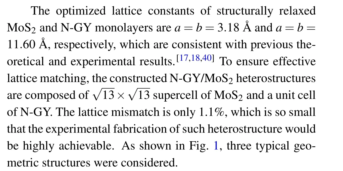
Fig.1. The top and side views of the optimized structure N-GY/MoS2 vdW heterostructures.
To assess the stability of the N-GY/MoS2 heterostructures, the binding energy (Eb) has been calculated using the definition

where theEN?GY/MoS2,EMoS2, andEN?GYare the total energy of the N-GY/MoS2heterostructures, MoS2, and N-GY layer, respectively. For the N-GY/MoS2heterostructures, the layer spacingd, binding energyEb, and thicknesshof MoS2are listed in Table 1. By comparison, the type-C heterostructure has the lowest binding energy of?0.497 eV, implying type-C stacking is the most stable structure. In the following discussion, we only consider type-C N-GY/MoS2heterostructures.As shown in Fig.1(C),the thicknessh(3.105 ?A-3.101 ?A)of MoS2layer in the N-GY/MoS2vdW heterostructure is slightly smaller than that in intrinsic monolayer MoS2(3.115 ?A), due to the compressive strain of MoS2during the formation of the heterostructures, which is similar to other vdW heterostructures.[41-43]
Table 1. Calculated interlayer spacing d,the thickness h of MoS2,and the binding energy(Eb)of N-GY/MoS2 vdW heterostructures.
In Figs. 2(a) and 2(b), the kinetic stability of N-GY and MoS2monolayer are confirmed by its phonon dispersion, where no imaginary phonon branches can be found. To check the dynamic stability of the heterostructures,ab initiomolecular dynamics(AIMD)simulations were performed using a 2×2 supercell containing 96 atoms at room temperature(300 K)for a total time of 9.6 ps with a controlled time step of 1 fs.The variation of energy and temperature with time during the simulation are shown in Fig.2(c).The amplitude of the oscillations in the total energy is relatively small,there is no significant deformation or bond breakage in the heterostructure,thus indicating that the heterostructure has a good thermodynamic stability.
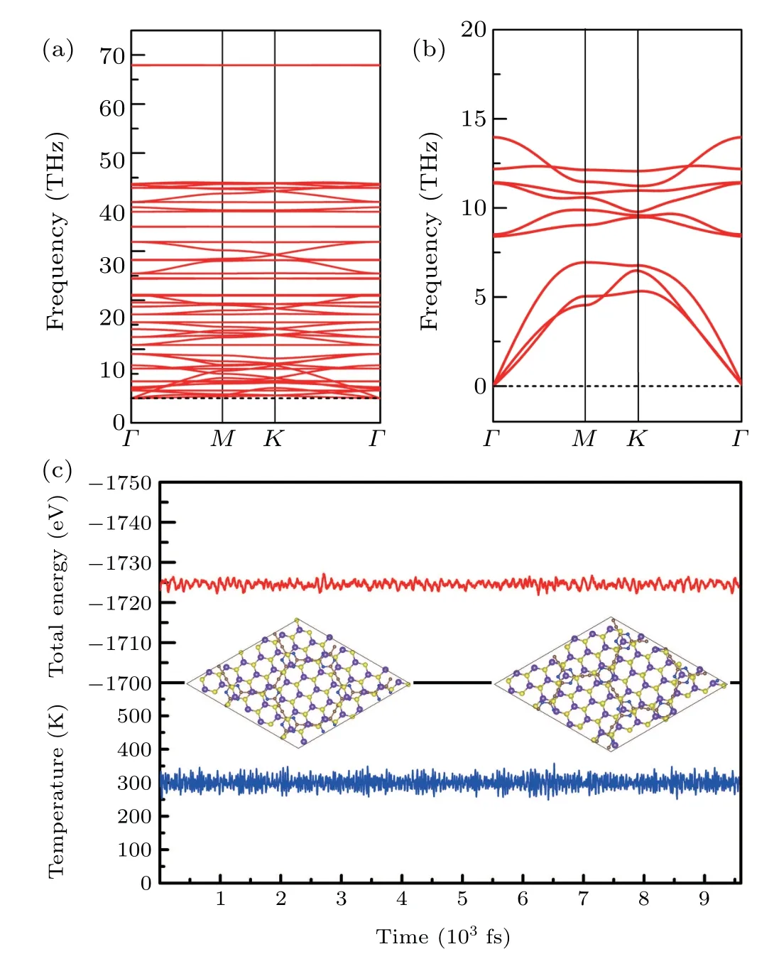
Fig.2. Phonon band structures of the(a)N-GY,(b)MoS2. (c)Variations of temperature and energy as a function of time for AIMD simulations of the N-GY/MoS2 vdW heterostructure.
3.2. Electronic properties
The band structures of the N-GY and MoS2monolayers are shown in Figs.3(a)and 3(b). The MoS2layer exhibits an indirect bandgap of 2.13 eV,while N-GY monolayer exhibits bandgap of 3.90 eV, which are agree with the experimental results.[44]As shown in Fig.3(a),the VBM and CBM are flat in N-GY layer, and the flat band appears due to Bloch phase extinction of the electrons in six-membered ring formed by the C and N atoms,where the electrons are tightly localized. The flat band is the opposite extreme to the Dirac band,where the intersection of conduction and valence bands exhibit a complete linear dispersion relationship,with massless and very fast electrons. In the flat band, the dispersion is zero, the kinetic energy of the electron is quenched, the effective mass is infinite and the density of states is very large.[41,45-49]
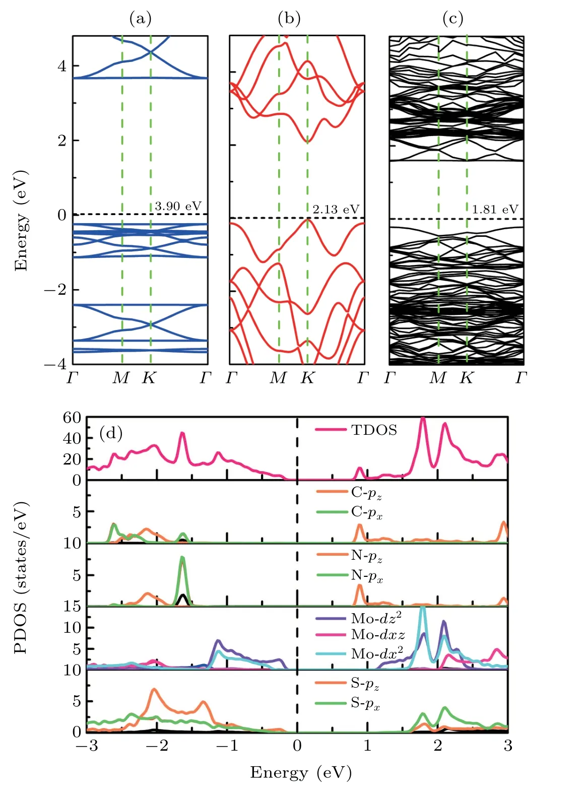
Fig. 3. The band structures of (a) N-GY, (b) MoS2, and (c) N-GY/MoS2 heterostructures. (d) The total and projected density states of N-GY/MoS2 heterostructures.
The electronic properties of the N-GY/MoS2heterostructure are presented in Fig. 3(c). The bandgap of the NGY/MoS2heterostructure is 1.81 eV.The projected density of states(PDOS)of the N-GY/MoS2heterostructure is shown in Fig. 3(d). From the PDOS, it can be observed that the CBM and VBM of the N-GY/MoS2heterostructures are contributed by N-GY layer and MoS2layer, respectively, which exhibits a typical type-II band alignment. The CBM is mainly contributed by the pzorbital electrons of the C and N atoms of the N-GY layer, which is the main source of the flat band. The VBM is contributed by the dz2orbital of the Mo atoms of the MoS2layer.
When different materials form a heterostructure, the difference in the work function causes a directional movement of electrons between the two layers.[16,25,50]The planar average electrostatic potentials along theZdirection for N-GY,MoS2layer, and N-GY/MoS2heterostructures are shown in Fig. 4.The work functions (Φ) of the N-GY and MoS2layer are 6.93 eV and 5.67 eV, respectively, which are consistent with previous reports.[2]The work function of the heterostructure is 5.52 eV,which are lower than that of the intrinsic monolayer N-GY and MoS2,respectively 1.41 eV and 0.15 eV smaller.
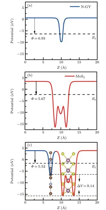
Fig.4.The average electrostatic potential for the N-GY monolayer(a),MoS2 monolayer(b),and N-GY/MoS2 heterostructures(c),respectively.
Due to the difference of work functions between N-GY layer and MoS2layer, the electrons spontaneously transfer from MoS2layer to N-GY layer until their Fermi levels are aligned.In the interface region,positive charges accumulate in MoS2layer and negative charges accumulate in N-GY layer,forming a built-inE-field (Eint), whose direction is directed from MoS2to N-GY layer.There is a potential drop of 9.14 eV in the N-GY/MoS2heterostructure. The potential drop can easily drive electrons from MoS2to N-GY,thus the concentration of holes in MoS2and the electron carrier concentration in N-GY can be amplified.
To better investigate the charge transfer mechanism at interfaces of heterostructures, in Fig. 5 we calculate the planeaveraged charge density difference (CDD), the CDD can be obtained by the following formula:
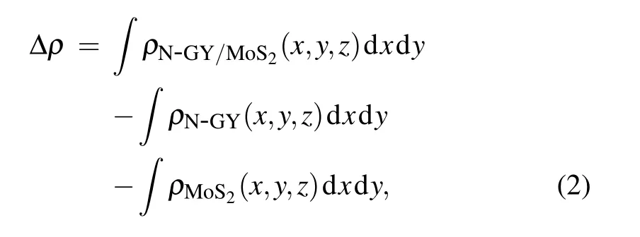
in the above equation,ρN-GY/MoSe2(x,y,z),ρN-GY(x,y,z),andρMoS2(x,y,z) are the charge densities of N-GY/MoS2heterostructures, MoS2, and N-GY layers, respectively. From Eq. (2), a positive value is defined as an accumulation of charge and a negative value represents the depletion of electric charges. As seen in Fig.5,the charges are redistributed at the interface of heterostructures, depleted in the N-GY layer(red) and accumulated at the S-atom position in the MoS2layer(cyan).The electron transfer number from MoS2layer to N-GY layer is 0.465e by Bader charge analysis.The charge rearrangement phenomenon generally leads to the formation of electron-hole depressions at the N-GY/MoS2heterostructures interface.[44]
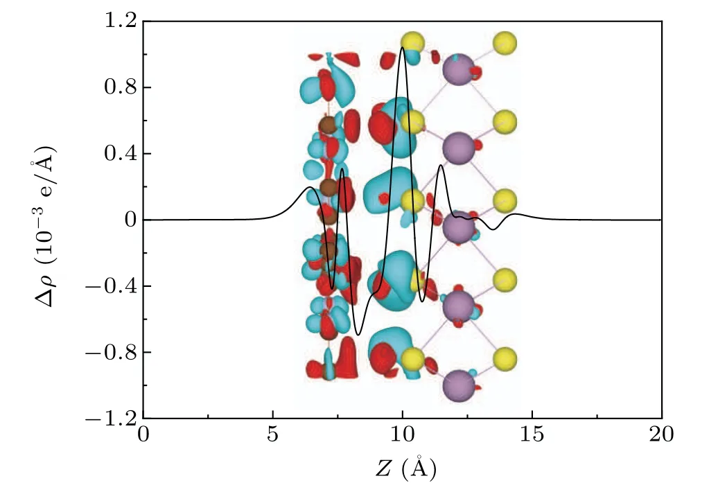
Fig. 5. The inset is the 3D isosurfaces of the charge density difference, the cyan and red areas represent charge accumulation and depletion,respectively,and the isosurfaces value is 0.0005 e/?A3.
3.3. Electric field effects on N-GY/MoS2 heterostructures
The adjustability of electronic structure is significant for the application of materials in electronic devices, and the external electric field (E-field) is an effective method for regulating the band alignment.[51]Figure 6(a) shows the relationship between the bandgap of N-GY/MoS2heterostructures and externalE-field. Here, we consider two externalE-field directions (+z,?z) perpendicular to the plane of heterostructure atoms. The positive direction is that the N-GY layer points to the MoS2layer, and the range is from?1.0 V/?A to 1.0 V/?A. When the +z E-field is applied, the bandgap of the heterostructures first increases and then remains unchanged,with the increase of theE-field strength, reaching the maximum value of 1.39 eV at theE-field=0.2 V/?A.The bandgap remains basically constant at theE-field of 0.2 V/?A-0.8 V/?A,because the direction of the externalE-field is opposite to theEintdirection in the heterostructures. The bandgap gradually decreases with theE-field strength further increasing.Conversely, when an external?z E-field in the same direction asEintis applied, the totalE-field is enhanced. The bandgap decreases further sharply with the externalE-field increase from 0 V/?A to?0.7 V/?A.Its bandgap could be zero atE-field>?0.7 V/?A, which suggests that the heterostructure could be tuned from semiconductor to metallic properties.
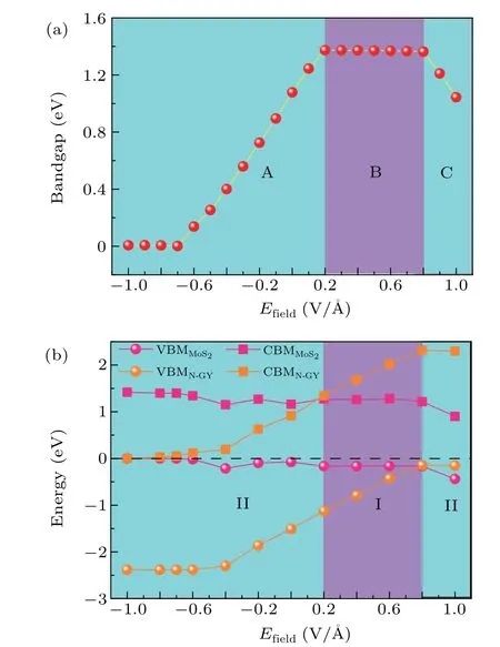
Fig. 6. The evolution of the bandgap (a) and the band edges (b) of the NGY/MoS2 heterostructures as a function of E-field.
The variation of band edges of N-GY/MoS2heterostructures under different externalE-fields are presented in Fig. 6(b). The CBM and VBM of MoS2in the heterostructures continue to move down with the increase of the positiveE-field strength,while the CBM and VBM of N-GY layer continue to rise. When the externalE-field=0.2 V/?A, the CBM of MoS2layer is lower than that of N-GY.Both the CBM and VBM of the heterostructures are contributed by the MoS2layer,and the system transforms into a type I band alignment.Notably, when the externalE-field>0.8 V/?A, the VBM of heterostructure is contributed by N-GY and the CBM is contributed by MoS2layer.At this time,the system is transformed into type-II band alignment again. With an increasing reverseE-field is applied to the heterostructure, the CBM and VBM of N-GY layer in the heterostructures continue to move down,while the CBM and VBM of MoS2continue to rise. At theEfield=?0.7 V/?A the CBM and VBM intersect, the bandgap is closed, thus the heterostructure could change from semiconductor to metal. The predicted results of this bandgap adjustment show that the electronic properties of the heterostructures can be effectively and dynamically controlled by the externalE-field, realizing the transition from type-II to type-I band alignment and from the semiconductor to metal.

Fig. 7. The integrated charge density difference of the N-GY/MoS2 heterostructures along the Z direction.
Furthermore, when an externalE-field is applied, the charge inside the heterostructure could be redistributed. The integrated charge density difference along theZdirection was calculated as
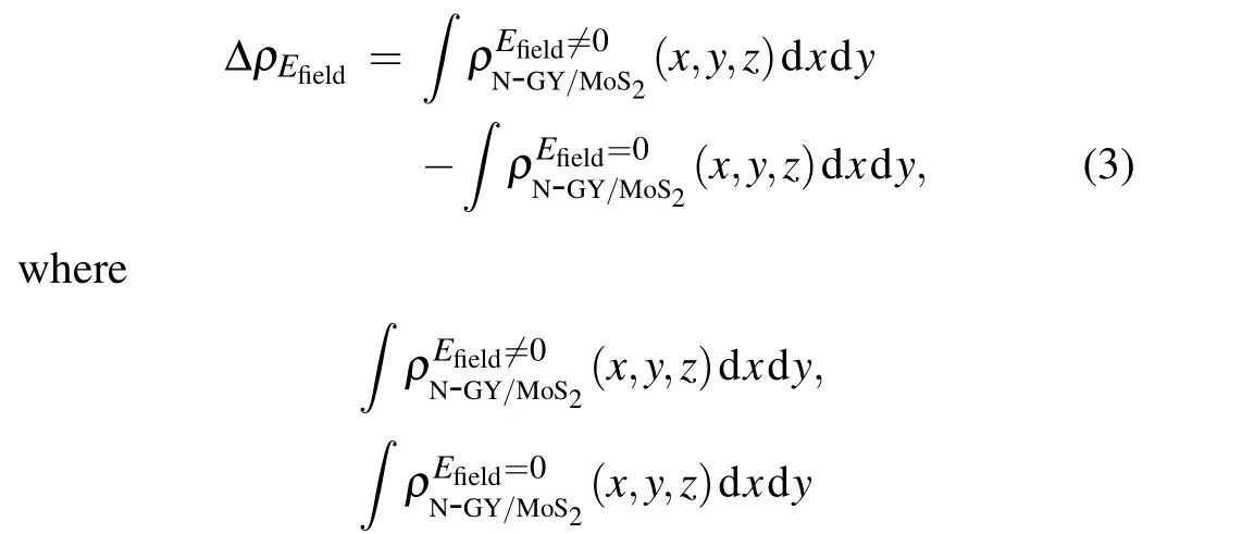
denote the charge density at the point in theZdirection for the heterostructures with and without an externalE-field, respectively. From the formula,a negative value indicates a depletion of charge and a positive value indicates an accumulation of charge. Figure 7 shows the planar average charge density along theZdirection for N-GY/MoS2heterostructures. The amount of charge transfer is proportional to the strength of the externalE-field and independent of the direction of externalE-field. Notably,a certain charge density also appears in the vacuum layer at largerE-field strengths due to dielectric breakdown and charge tunneling, which is similarly observed for the arsenic/C3N,blue phosphorus/C2N,and Sb/InSe heterostructures.[52-54]
3.4. Strain effects on N-GY/MoS2 heterostructures
Biaxial strain is one of the effective ways in which the electronic structure of layered materials can be tuned. Figure 8(a)illustrates the bandgap as a function of biaxial strain(ε=?4%to 4%). The biaxial strain is defined asε=?l/l×100%, where ?landldenote the change in lattice constant and the intrinsic lattice constant, respectively. When tensile strain is applied to the system,the bandgap of the heterostructures monotonically decreases. With compressive strains are applied,the bandgap of the heterostructure increases and then decreases, reaching a maximum of 1.19 eV atε=?2%.The variations of the band alignment of the N-GY/MoS2heterostructures with strains are presented in Fig.8(b). From 0%to?4%of strains,the CBM of MoS2shifts upwards with increasing strains,but is always higher than the CBM of N-GY layer. At this point,the VBM of heterostructure is contributed by MoS2, the CBM is contributed by N-GY, and the system shows a type-II band alignment.When tensile strain is applied,the CBM of MoS2moves down with the increase of strain. At theε=2%, both VBM and CBM of the heterostructures are contributed by MoS2,and the system is transformed into type-I band alignment. The above results show that biaxial strain can effectively regulate the band structure of heterostructures to achieve the transition from type-II to type-I band alignment.
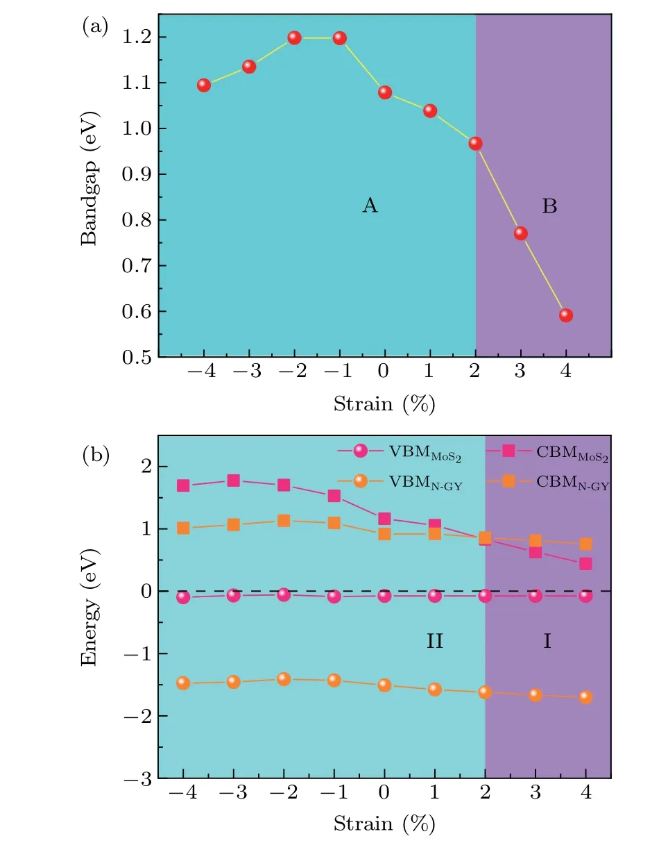
Fig. 8. The evolution of the bandgap (a) and the band edges (b) of NGY/MoS2 heterostructure as a function of strain.
3.5. Optical properties
The optical absorption coefficients of the N-GY/MoS2heterostructures are presented in Fig. 9. The optical absorption coefficient is defined by the following equation:
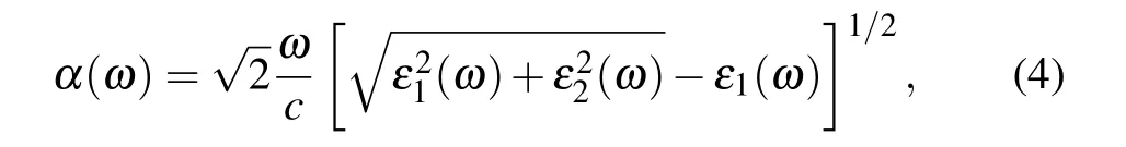
whereε1(ω)andε2(ω)are the real and imaginary parts of the complex dielectric function,respectively. The first absorption peak of the intrinsic N-GY layer is in the UV region and the absorption coefficient is almost zero in the visible range. The N-GY/MoS2heterostructures can break through the restrictions of isolating layer and combine their optical absorption strength together. The N-GY/MoS2heterostructure is found to absorb a wide range of solar spectrum in the visible region as compared to the constituent monolayers. In the UV-visible light the optical absorption coefficient is 105cm?1,the type-II band alignment facilitates exciton-hole complexation and increases exciton lifetime. Good absorbance is essential for its performance in optoelectronic and photovoltaic applications.By comparing the band edges of monolayers forming type-II band alignment, the application prospect of this heterostructure in 2D exciton solar cell is prospected.
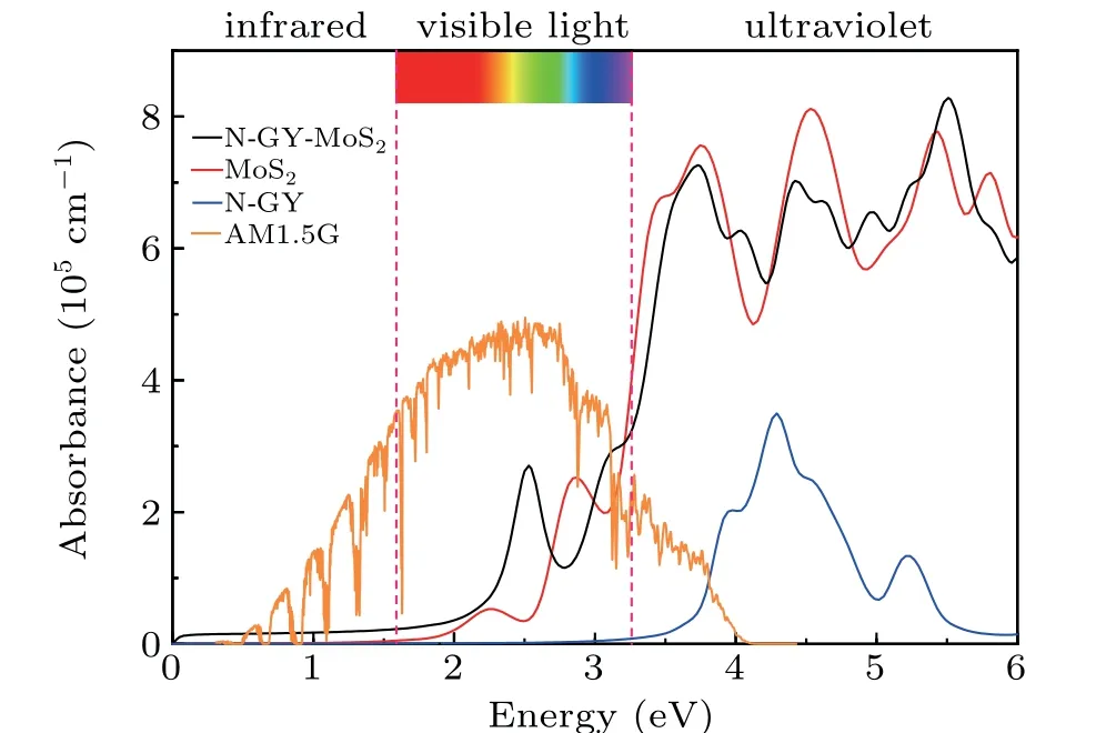
Fig. 9. Optical absorption coefficients of MoS2, N-GY, and N-GY/MoS2,heterostructures at the HSE06 level.
The power conversion efficiency (PCE) of N-GY/MoS2heterostructures can be evaluated as[55]
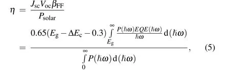
where 0.65 is the band-fill factor (βFF),Egis the bandgap of the donor, and the term (Eg??Ec?0.3) evaluates the maximum open-circuit voltageVoc. TheP(?ω)is the air mass 1.5(AM1.5)solar energy flux at the photon energy ?ω.EQE(?ω)is the external quantum efficiency and is assumed to 100%.The integral in the numerator depicts the short-circuit currentJscin the limit of 100%EQE(?ω) while the denominator is the solar energy flux at AM1.5. The calculated PCE for the intrinsic N-GY/MoS2heterostructures is 17.77%,which is comparable to the recently reported, such as phosphorene/MoS2(18%-21%)[56]and GeSe/SnS heterobilayers(~18%).[57]As shown in Fig. 10(b), we design the N-GY/MoS2heterostructures as a solar cell with Au and ITO as electrode material,N-GY layer as the acceptor and the MoS2layer as the donor,respectively.

Fig. 10. (a) The power conversion efficiency of N-GY/MoS2 heterostructures. (b)Schematic illustration of the thin-film solar cell.
4. Conclusion
In summary, density functional theory calculations were performed to systematically study the electronic and optical properties of the N-GY/MoS2heterostructures. The binding energy and molecular dynamics simulations demonstrate that N-GY/MoS2van der Waals heterostructures could exist stably. The externalE-field and biaxial strain can effectively adjust the bandgap and band edge positions, converting the heterostructures from type-II to type-I band alignment. The bandgap of the heterostructures varies in trend under different externalE-fields, varying linearly in the range of?0.7 V/?A to 0.2 V/?A and 0.8 V/?A to 1.0 V/?A,but remaining essentially constant in the range of 0.2 V/?A to 0.8 V/?A.The charge transfer is proportional to the strength of externalE-field. In addition, the heterostructure exhibits an excellent optical absorption coefficient of 105cm?1, range from visible to UV. The power conversion efficiency of N-GY/MoS2heterostructure is high to 17.77%,suggesting this heterostructure is a promising candidate for solar cells. Our work shows that N-GY/MoS2heterostructure is a candidate material for semiconductor sensors and photovoltaic devices due to effective charge separation,tuned band alignment,broad optical absorption spectrum,high optical absorption intensity, and high power conversion efficiency.Acknowledgment
The authors thank the high performance computing center of Henan Normal University.
猜你喜歡
中學生數理化·高一版(2022年4期)2022-05-09
思維與智慧·上半月(2022年4期)2022-04-08
中國棉花(2021年5期)2021-01-02
東坡赤壁詩詞(2020年3期)2020-07-04
軟件(2020年3期)2020-04-20
Chinese Physics B(2019年10期)2019-11-06
中學生理科應試(2019年3期)2019-07-08
中學生數理化·高二版(2017年3期)2017-07-07
中學生數理化·中考版(2016年10期)2016-12-22
中學生數理化·高二版(2016年9期)2016-05-14
- Chinese Physics B的其它文章
- Numerical investigation on threading dislocation bending with InAs/GaAs quantum dots*
- Connes distance of 2D harmonic oscillators in quantum phase space*
- Effect of external electric field on the terahertz transmission characteristics of electrolyte solutions*
- Classical-field description of Bose-Einstein condensation of parallel light in a nonlinear optical cavity*
- Dense coding capacity in correlated noisy channels with weak measurement*
- Probability density and oscillating period of magnetopolaron in parabolic quantum dot in the presence of Rashba effect and temperature*