
Abnormal phenomenon of source-drain current of AlGaN/GaN heterostructure device under UV/visible light irradiation*
2021-11-23 07:30YueBoLiu柳月波JunYuShen沈俊宇JieYingXing邢潔瑩WanQingYao姚婉青HongHuiLiu劉紅輝YaQiongDai戴雅瓊LongKunYang楊隆坤FengGeWang王風格YuanRen任遠MinJieZhang張敏杰ZhiShengWu吳志盛YangLiu劉揚andBaiJunZhang張佰君
Chinese Physics B 2021年11期
Yue-Bo Liu(柳月波) Jun-Yu Shen(沈俊宇) Jie-Ying Xing(邢潔瑩) Wan-Qing Yao(姚婉青)Hong-Hui Liu(劉紅輝) Ya-Qiong Dai(戴雅瓊) Long-Kun Yang(楊隆坤)Feng-Ge Wang(王風格) Yuan Ren(任遠) Min-Jie Zhang(張敏杰)Zhi-Sheng Wu(吳志盛) Yang Liu(劉揚) and Bai-Jun Zhang(張佰君)
1School of Electronics and Information Technology,Sun Yat-sen University,Guangzhou 510006,China
2State Key Laboratory of Optoelectronic Materials and Technologies,Sun Yat-sen University,Guangzhou 510275,China
Keywords: AlGaN/GaN heterostructure,two-dimensional electron gas(2DEG),surface states,irradiation
1. Introduction
AlGaN/GaN heterostructure devices have potentials in fields of high-power electronics and high frequency electronics.[1-6]The advantages of AlGaN/GaN heterostructure comes from characteristics of high-electron mobility due to the two-dimensional electron gas (2DEG), which is induced by the positive polarization charges at heterostructure interface.[7]Although the structure has many advantages, it also brings some problems to solve.A large number of defects and traps in the AlGaN/GaN materials would damage the stability and efficiency of AlGaN/GaN devices.[8-10]The surface states, decided by the distribution of defects and traps on the surface, have great impact on the electrical characteristic of semiconductor devices.[11,12]The light irradiation can change the surface states, which affects the characteristics of Al-GaN/GaN heterostructure devices. In 2000,Elhamriet al.[13]found the extended illumination of a blue GaN-based LED resulted in an increase in the carrier density and a decrease in the mobility of an AlGaN/GaN heterostructure.In 2003,Mizutaniet al.[14]found that the surface states can capture electrons injected from the gate and resulted in the drain current collapse in AlGaN/GaN HEMTs, but the collapse can be suppressed by light illumination with energy smaller than the bandgap.In 2006, Okadaet al.[15]reported that the blue LED and incandescent lamp can lead to a large threshold voltage shift in AlGaN/GaN HFETs,but the red LED illumination almost cannot change the threshold voltage. In 2007 and 2010,Changet al.[16,17]reported that the channel resistance increases when the device is illuminated with subbandgap energy photons after the UV-induced variation becomes stable. The reason is the positively charged surface states captured of excess electrons. In 2012,Fagerlindet al.[18]found that the illumination of photons with energies between 3.1 and 3.7 eV can lead to decay of persistent photoconductance GaN/AlGaN/GaN heterostructure materials due to the delayed recombination between electrons emitted from surface states and the deep level states in the AlGaN layer. In 2016, Lianget al.[19]reported that light illumination can accelerate recovery of the current collapse after the field stresses in AlGaN/GaN HEMTs. In 2020,Nagarajanet al.[20]reported that the 365 nm UV can improve the current dispersion in AlGaN/GaN HEMTs. In this work,we report the abnormal phenomenon about the decrease of theIDunder visible light irradiation for the AlGaN/GaN heterostructure device. However, the current increases under 390 nm light,whose photon energy is less than the band gaps of GaN and AlGaN. This abnormal phenomenon appeared during the testing of the device stability, then we conducted a series of experiments to reveal the generation mechanisms of these physical phenomena. We speculate that the abnormal phenomenon is related to the surface barrier height,which is decided collaboratively by the surface states and polarization effect of AlGaN/GaN materials. To make the abnormal phenomenon clear, a series of experiments about irradiation have been completed. The physical mechanisms leading to the abnormal phenomena have been analyzed based on the experimental results and the technology computer aided design(TCAD)simulation results. This work has revealed the effect of the UV/visible light irradiation and the surface states on the stability of AlGaN/GaN heterostructure devices.
2. Experimental details and results
The AlGaN/GaN heterostructure samples were grown on Si (111) substrates by a metal organic chemical vapor deposition (MOCVD) system, the epitaxial structure of the device consists of an AlN seeding layer, a GaN buffer layer(5.0 μm), an undoped GaN channel layer (200 nm), and an Al0.35Ga0.65N barrier layer (25 nm). The sheet carrier concentration and mobility of AlGaN/GaN samples are 3.45×1012cm?2and 1268 cm2/V·s by Hall measurement at room temperature,respectively.
To eliminate the impact of the conventional metal gate and the probes on the incident light irradiation, the device used in experiments was designed to a gateless structure with two metal lines. The detailed structure of device is illustrated in Figs.1(a)-1(c). In the course of the experiment, the probes placed on the pads can be connected to the device by the metal interconnection lines, so the incident light irradiation can reach the surface of AlGaN/GaN heterostructure directly. The gateless device was fabricated with the following process. Firstly, a mesa structure of 100 nm thickness and 840×520 μm2area was etched by the inductively coupled plasma reactive ion etching (ICP-RIE) system. Then,Ti/Al/Ni/Au (50/200/40/40 nm) were deposited by electron beam evaporation to form the source and the drain electrodes with 800μm long,100μm wide and separated by a distance of 300μm. Ohmic contacts of the source and the drain electrode were formed by rapid thermal annealing(RTA)at 850°C for 30 s in nitrogen ambient. Thirdly, Ti/Au (15/100 nm) metals were deposited to form the metal interconnection lines and the testing pads.
The rocking curve of the AlGaN/GaN heterostructure has been shown in Fig. 1(d), which is obtained by x-ray diffractometry(XRD)measurement.The full width at half maximum(FWHM) is 0.17547°. The dislocation density can be evaluated as follows:[21]
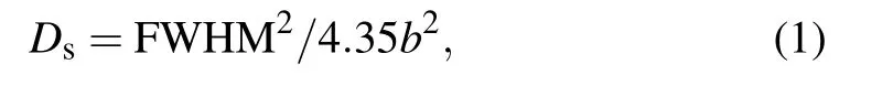
wherebis the length of the Burger vector and the unit of the FWHM is radian. Thus, the dislocation density is 8.02×108cm?2.
The density of surface states on the bare surface of the Al-GaN/GaN heterostructure cannot be measured directly,but the density of surface states under a Schottky contact can be obtained by calculation. In general,the density of surface states under a Schottky contact far less than the density on a bare surface. The current in Schottky barrier diodes can be expressed as
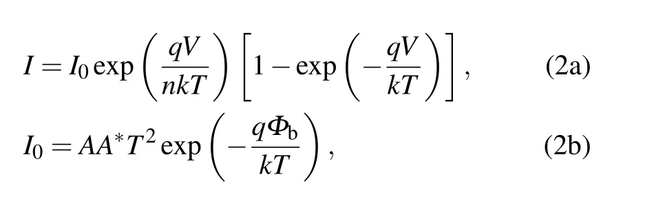
whereI0is the saturation current;Ais the area of the Schottky contact;A*is the Richardson constant of AlGaN,its value is 32.4 A·cm?2·K?2;nis the ideal factor;Φbis the Schottky barrier height. Thus,the ideal factor and the Schottky barrier height of the Schottky barrier diode are 1.56 and 0.79 eV,respectively.
For n-type Schottky contacts,the Schottky barrier height can be expressed as[22]
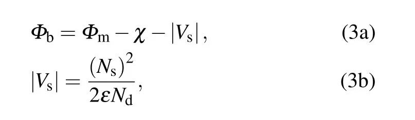
whereΦm=5.2 eV is the work function of Ni;χ=1.9 eV is the electron affinity of Al0.35Ga0.65N;[23]|Vs|is the surface band bending energy;εis the permittivity of Al0.35Ga0.65N;Ndis the carrier concentration in the AlGaN/GaN heterostructure. Thus,the density of surface states under a Schottky contact is 1.10×1010cm?2.
Therefore,the density of surface states on the bare surface is much larger than the dislocation density.
In the experiments, a device analyzer (Agilent B1500A,Santa Rosa, CA, USA) was applied to measure the electrical characteristics of AlGaN/GaN heterostructure device at room temperature. The drain currentID-time curves of the AlGaN/GaN heterostructure device was measured under light irradiation or in the dark environment. To eliminate the possible interference factors,a sufficient recovery time was adopted between two tests. The LED lamp with different wavelengths was used as the light irradiation source. The central wavelengths of LED lamps are 620 nm,590 nm,520 nm,470 nm,390 nm,365 nm and 280 nm,respectively.
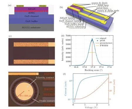
Fig.1.The cross-sectional side view(a)and vertical side view(b)of an AlGaN/GaN heterostructure device.(c)Optical microscope photograph of the mesa part. (d) The rocking curve of the AlGaN/GaN heterostructure in XRD measurement. (e) Optical microscope photograph of a Schottky barrier diode based on the AlGaN/GaN heterostructure. (f)The I-V curve of the Schottky barrier diode.
Before the measurements, in order to enable the excited electrons relaxation back to the bound states,AlGaN/GaN heterostructure devices were placed in the dark box for one night.
In general, when the energy of the irradiated photon is larger than the band gap of the material,the photon will be absorbed resulting in photogenerated carriers, which causes the rise of the current. However,when the energy of the irradiated photon is less than the band gap of the material, the photon will not be absorbed and will not cause the change of current.Even if such photons can excite carriers on the unionized impurity states and generate photogenerated carriers,the current will rise.However,an anomalous phenomenon of current drop was observed in our experiments.
The curve ofIDversus time is shown in Fig.2. The solid line indicates the time period in dark, and the dotted line indicates the time period under light irradiation. Before turning on the LED lamps,the drain voltage(VDS)fixed at 0.5 V was applied.IDshows a stable value of 510 μA, which is determined byVDSand the resistance of 2DEG channel. When the LED lamp is turned on,IDshows different trends according to the wavelength of LED lamp. Similarly,when the LED lamp is off,IDalso shows different trends.
As shown in Fig. 2(a), the device was irradiated by the visible LED lamp, and its wavelengths are 620 nm, 590 nm,520 nm,470 nm,respectively.When the LED lamp was turned on,IDshows an obvious decrease. The amplitude of the decrease may be related to light intensity and wavelength.An increase ofIDwas observed when the light was off. By contrast,as the wavelength decreases, the phenomenon ofIDdecline does not appear, but rises, even its photon energy is less than the band gaps of GaN and AlGaN.As shown in Fig.2(b),IDincreases significantly when irradiated under UV LED lamps with the wavelengths of 390 nm, 365 nm, 280 nm light, respectively. A current drop was observed in theID-time curve when the light was off.
To further investigate the abnormal phenomenon, we turned on the UV LED lamp with 280 nm light,IDincreased swiftly. On the basis of this condition,we turned on the LED lamps with wavelengths of 390 nm,470 nm,520 nm,590 nm,and 620 nm, respectively. TheID-time curves are shown in Fig.2(c). The solid line indicates the time period only the irradiation of under 280 nm light, and the dotted line indicates the time period under the irradiation of two LEDs’ lights simultaneously. Although the decrease amplitude of the current is small,the decrease of theIDcan still be observed when the LED lamp is turned on except the LED lamp with 390 nm light.
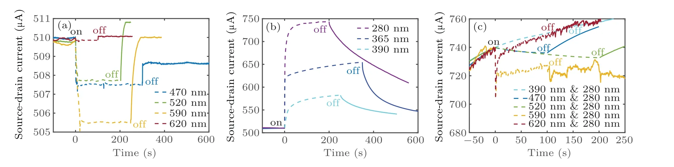
Fig.2. (a)The ID-time curves under 620 nm,590 nm,520 nm,470 nm light. (b)The ID-time curves under 390 nm,365 nm and 280 nm light. (c)The ID-time curves under two lights simultaneously,with one at 280 nm,and the other in turn at 620 nm,590 nm,520 nm,470 nm,and 390 nm.
3. Physical mechanism and discussion
In wurtzite III-V nitrides materials, the strong polarization electric field originates from spontaneous polarization(SP) and piezoelectric polarization (PE). SP is the inherent properties of wurtzite III-V nitride materials, and PE comes from the lattice mismatch at the interface. The abrupt change of polarization at AlGaN/GaN heterointerfaces results in the interface polarization charge.In the[0001]direction,the component of polarization along thec-axis plays a crucial role,which can be expressed by the material mole-fraction and lattice parameters as[7,24,25]
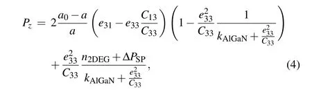
where ?PSPequals the spontaneous polarization of GaN minus the spontaneous polarization of Al0.35Ga0.65N;n2DEGis the density of the 2DEG;kAlGaNis the permittivity of AlGaN material;a0andaare the lattice constants of GaN and AlGaN materials,respectively;ei jis the piezoelectric coefficient,andCi jis elastic constant. Equation (4) has been widely used in the simulation for the polarization charges.The parameters for wurtzite III-V nitride materials used are listed in Table 1.[26]
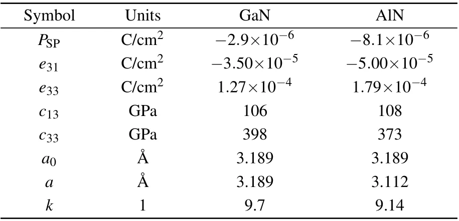
Table 1. Parameters for polarization model used in calculation.
The model parameters of AlGaN are determined by mole fraction, calculated by the values of linear interpolations between parameters of GaN and AlN.
The charge distribution can be obtained by fully coupled form of the Poisson equation as follows:[24,27]
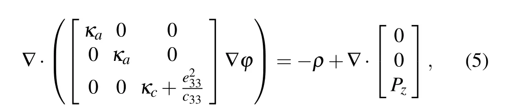
whereκiis the second-ranked permittivity tensor. The anisotropic Poisson equation (5) has been used in the simulation for calculating the carrier distribution in AlGaN/GaN heterostructure.
The 2DEG originates from large quantities of donorlike surface states, which is the most widely accepted explanation.[28-30]The distribution of surface surface states plays an important role on the physical characteristics of Al-GaN/GaN heterostructure. Two kinds of surface barrier, the fixed surface barrier and the variable surface barrier height from 1.0 to 1.8 eV have been reported.[12,31]In a report, the surface barrier height will be fixed when the surface-state density is on the order of 1×1014cm?2·eV?1or higher.[32]The above experimental results show that the lights with various wavelengths can affect theID. This means that the variable surface barrier height model is consistent with the actual experimental results. The distribution of surface states is still unclear,so we approximatively assume a simple uniform distribution model of surface states in this study. The surface donor-like states are continuously distributed from the Fermi level to the bottom of the conduction band with a fixed finite densitynin units of cm?2·eV?1. Under the condition that the surface barrier heightΦsis higher than critical surface barrier heightΦc,the density of the 2DEG can be represented as[32]It means that the distribution of surface states is directly related to the surface barrier height,the two parameters present a negative correlation on the same thickness and molar fraction of AlGaN premise.
Equations(4)-(6)constitute the physical model of the Al-GaN/GaN heterostructure,which can be used in simulations to calculate the surface barrier height,surface barrier height and the the carrier distribution in AlGaN/GaN heterostructure.
The barrier height on surface and the density of 2DEG is related to the density of surface states. The relationship between them is shown in Fig. 3, which is obtained from the simulation.
The photon energies of 390 nm and 470 nm light are both less than the bandgaps of GaN or AlGaN.In the experiments,the irradiation of 390 nm light increases theIDof the device,but 470 nm light decreases the current under the same condition. We speculate that the difference between the two results depends on the surface barrier height. According to the experimental data, the surface barrier height should be between 2.64 eV(photon energy of 470 nm light)and 3.18 eV(photon energy of 390 nm light).
The energy level structure,the charge distribution and the physical processes under various light irradiations are present in Fig.3. We assume that the surface states on the AlGaN surface are completely ionized between the bottom of conduction band and the Fermi level. However,the surface states located below the Fermi level are all filled with charge. Figure 3(a)shows the energy level structure and the charge distribution under the dark condition.
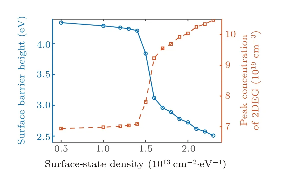
Fig. 3. The relationship between the surface states density, the barrier height and the peak concentration of 2DEG.
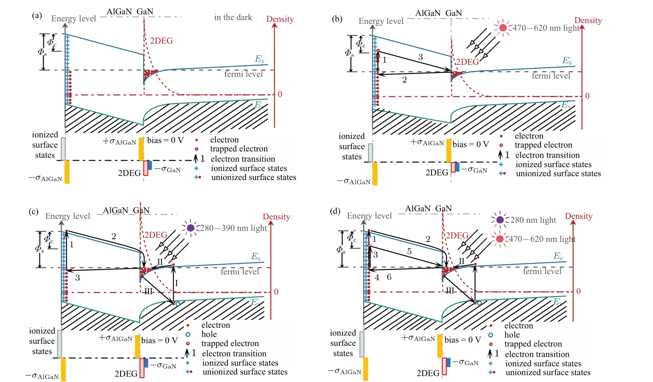
Fig.4. Schematic energy level structure, the charge distribution, and physical processes(a)under the dark condition, (b)under 470-620 nm light irradiation,(c)under 280-390 nm light irradiation,and(d)under 280 nm and 470-620 nm light irradiation simultaneously.
The physical process under the visible light irradiation with wavelengths of 470 nm, 520 nm, 590 nm and 620 nm is present in Fig. 4(b). The photon energies of these visible lights are less than the surface barrier height, which cannot excite electrons in unionized donor-like surface states under the Fermi level to transit to conduction band of the Al-GaN layer. The excited electrons were trapped by the ionized donor-like surface states above the the Fermi level,as the step 1 in Fig.4(b). The trapped electrons have relatively long lifetimes. The newly ionized donor-like surface states near the Fermi level can obtain electrons from 2DEG by tunneling, which causes the decrease of electron density in 2DEG channel,as the step 2 in Fig.4(b). In addition,the trapping of excited electrons by the ionized donor-like surface states will cause the polarization field to weaken, which further leads to the decrease of electron density in 2DEG channel. In macroscopic view, it manifested as the decrease of theID. If the surface states above the Fermi level are fully occupied, theIDwould be zero. Because the electrons in 2DEG originates from the donor-like surface states,[12,28,29]the fully occupied surface states and the the negative polarization charges at the surface would reduce the depth of triangular potential well at the AlGaN/GaN interface and make the 2DEG disappear,but it never happened in the experiments. The result of TCAD simulations also indicates that only a small part of surface states in barrier are occupied under the irradiation within the scope of 470 nm to 620 nm light. After the end of irradiation, the trapped electrons would be released and tunnel into the 2DEG,then the current recovers,as the step 3 in Fig.4(b).
Of course, the light irradiation can also excite the electrons bound by the AlGaN/GaN interface states,but the Fermi level at the interface is close to the bottom of the conduction band,the excited electrons can easily leap into the conduction band and jump to 2DEG channel quickly,which will not cause theIDto decrease.Furthermore,the excited electrons may also be trapped by the defects inside the AlGaN layer. The density of dislocation in AlGaN is much less than the density of the surface states, so the surface states dominate the process.Therefore,the possible process about the defects is not shown in Fig.4(b). We believe that the abnormal phenomenon is related to the surface states of AlGaN rather than the interface states located at AlGaN/GaN interface.
Figure 4(c) indicates the physical process under the UV light irradiation with the wavelength of 390 nm, whose photon energy is greater than the surface barrier height and less than the band gap of GaN.It can excite the electrons in unionized donor-like surface states near the Fermi level to transit to the conduction band and leaves the newly ionized donorlike surface states, as the step 1 in Fig. 4(c). These electrons transit to the conduction band drift rapidly to the AlGaN/GaN interface and jump into 2DEG channel under the polarization electric field, which cause the increase of electron density in 2DEG channel,as the step 2 in Fig.4(c). The greater density of 2DEG leads to the increasing current. These ionized donorlike surface states can enhance the polarization electric field.After the irradiation ends, the current recovers, as the step 3 in Fig. 4(c). When the wavelength of UV light is 365 nm or 280 nm, whose photon energy is greater than surface barrier height and the band gap of GaN.The photons can be absorbed directly by the GaN buffer,and lots of electrons in the valance band can be excited to increase theID.This process may dominate the increase ofIDand has been shown in the steps I and II.After the irradiation ends,the current recovers,as the step III.
For the case of the device irradiating under 280 nm UV light and another wavelength light together, the physical process includes the above two cases,which can be explained by them, as depicted in Fig. 4(d). The physics process under the irradiation of 280 nm and 390 nm light is similar, so the 390 nm light can affect the device slightly under the continuous irradiation of 280 nm light.
The electrons trapped in the ionized donor-like surface states show a long relaxation time. The lifetime of electrons,which were excited by different wavelength visible lights and trapped in the ionized donor-like surface states, was obtained by using the experimental data in Fig.2(a)and the equation as follows:[17]
The first term on the right side of the equation relates to the current recovery characteristics, and the second term relates to the background currents. The parameterτis the average lifetime of the trapped electrons. Theτ'is a constant associated with the rate of background current gain.Ais a constant associated with the amplitude attenuation of current.A'is a constant associated with the amplitude gain of background current.The experimental data points and the fitting curves are shown in Fig.5. The discrete geometry elements indicate the experimental data, and the curves indicate the fitting results.The fitting curves agree with the experimental data very well.The inset shows the experimental data and the fitting results of 470 nm and 620 nm light. Only a few data can be obtained for 470 nm and 620 nm light due to the minimum interval of the test time of 0.5 s. AlthoughR2is very close to 1,it could still lead to the imprecise results.
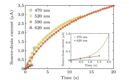
Fig.5. The experimental data and the fitting curves of 470 nm,520 nm,590 nm, and 620 nm light. The experimental data were obtained from Fig. 2(a) in the recovery period of each curves. The inset shows the experimental data and the fitting curves of 470 nm and 620 nm light.
The fitting results are listed in Table 2. The average lifetimes of the trapped electrons excited by 520 nm and 590 nm light are much longer than that of the trapped electrons excited by 470 nm and 620 nm light, which probably means that the types of surface states at different energy levels are great different. The existence of the trapped electrons average lifetime supports the physical mechanisms of the above-stated abnormal phenomena.

Table 2. Summaries of fitting parameters, the current recovery at the end of various irradiation.
In order to further explain the physical mechanism of the abnormal phenomenon, the density of the trapped electrons or the occupied surface states at AlGaN surface under 620 nm,590 nm,520 nm,470 nm light irradiations were simulated by TCAD, respectively. In the simulation, the physical model involves the polarization,crystallographic direction,fully coupled form of Poisson’s equation,the uniform distribution model of surface states,Shockley-Read-Hall recombination and the trapped electrons. The experimental results show that the barrier height on the bare surface of AlGaN is in the range from 2.64 eV to 3.18 eV.The numerical simulation results indicate that the density of the uniform distribution model of surface states,nis in the range from 1.6×1013cm?2·eV?1to 2.1×1013cm?2·eV?1. For convenience of calculations,we assign a value ton,1.8×1013cm?2·eV?1,which corresponds to the surface barrier height of 2.89 eV. Then the fixed negative charges are introduced as the trapped electrons in simulation.Neis the sheet concentration of the trapped electrons on surface, in units of cm?2. By changing the value ofNe, the electron density of 2DEG irradiated under 470 nm, 520 nm,590 nm,and 620 nm light were simulated,respectively.
Figure 6(a)shows the energy band structure near the heterostructure on 0.5 V drain voltage, in the dark, 470 nm,520 nm,590 nm,620 nm light irradiations,respectively. The solid lines indicate the conduction bands, the chain-dotted lines indicate the quasi-fermi level of electron,and the dashed lines indicate the valence bands. The inset illustrates the full view of the energy band structure.Figure 6(b)shows the distribution of electron density on 0.5 V drain voltage,and the inset illustrates the distributions of electron density around the peak.As shown in Fig. 6(b), the irradiations of 470 nm, 520 nm,590 nm, 620 nm light can directly decrease the peak of electron density of 2DEG.It leads to the abnormal phenomenon of theID.
The simulation results are listed in Table 3.Neis far less thann, which means that only a small part of surface states in the barrier can be occupied under the visible light irradiations within the scope of 470-620 nm. Under the different light conditions, the densities of the trapped electronsNeare different,as listed in Table 3. Because the material structure is fixed,the Poisson equation(5)and Fig.3 indicate that theΦsis determined by the density of the surface states and theNe.Hence,theNeand theΦsboth change with the wavelength of lights.
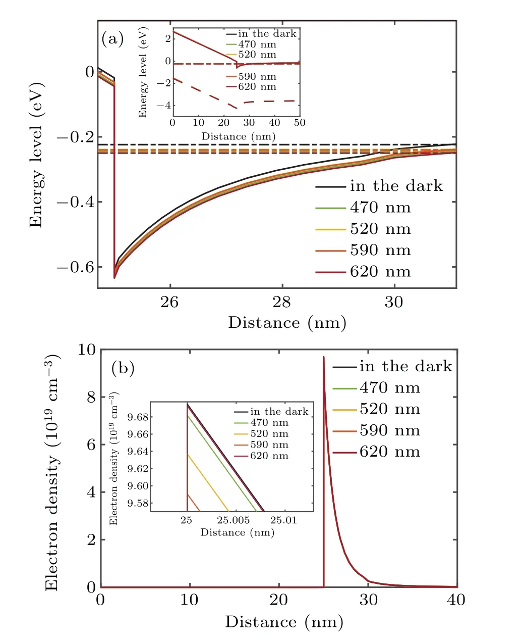
Fig.6. (a)The energy band structure near the heterostructure on 0.5 V drain voltage. The inset shows the full view of energy band structure.(b)The distribution of electron density on 0.5 V drain voltage.The inset illustrates the distributions of electron density around the peak.
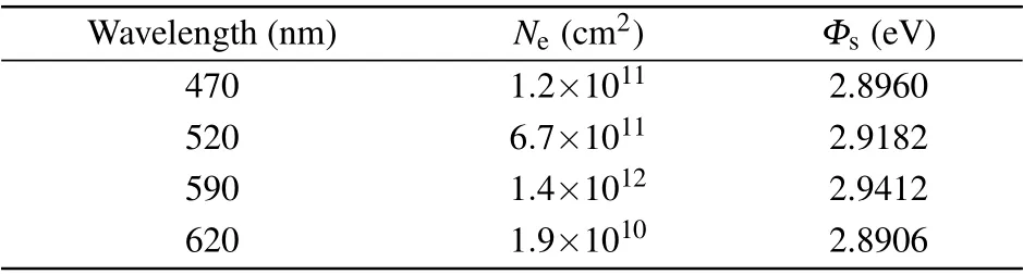
Table 3. Simulation results,the sheet concentration of the trapped electrons,and the corresponding surface barrier height.
The relations among the injection current, optical output power and rate of photon generation are shown in Fig.7. The optical powers and rates of photon generation of the different lights are different in same injection currents. The optical power and rate of photon generation of the 590 nm light are both the lowest. However, as shown in Fig. 2, the 590 nm light can bring the maximum reduction of theID. In the experiment, the injection currents of LEDs are staying at 500 mA.As shown in Table 3, the amount of the trapped electrons on surface is much less than the number of photons generated in a second,so the reductions of theIDin 620 nm,590 nm,520 nm and 470 nm lights would change slightly when the injection currents are in the range of 100 mA to 700 mA.
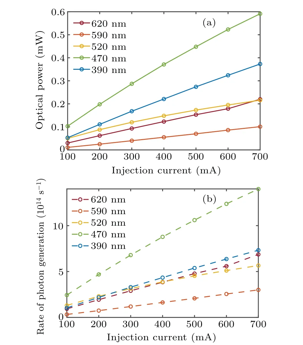
Fig. 7. (a) The relations between the injection current and the optical output power. (b) The relations between the injection current and the rate of photon generation.
4. Conclusion
An abnormal phenomenon of source-drain current in Al-GaN/GaN heterostructure devices induced by UV/visible light irradiation is observed in our experiments.We propose a physical model to explain this abnormal phenomenon in detail. We believe that the abnormal phenomenon is related to the surface states of AlGaN rather than the interface states located at AlGaN/GaN interface because the Fermi level at the interface is close to the bottom of the conduction band. The simulation results are in good agreement with the experimental data. The research on the physical mechanism of the abnormal phenomenon will take an important role on the stability of AlGaN/GaN heterostructure devices.
- Chinese Physics B的其它文章
- Numerical investigation on threading dislocation bending with InAs/GaAs quantum dots*
- Connes distance of 2D harmonic oscillators in quantum phase space*
- Effect of external electric field on the terahertz transmission characteristics of electrolyte solutions*
- Classical-field description of Bose-Einstein condensation of parallel light in a nonlinear optical cavity*
- Dense coding capacity in correlated noisy channels with weak measurement*
- Probability density and oscillating period of magnetopolaron in parabolic quantum dot in the presence of Rashba effect and temperature*