
Low working loss Si/4H-SiC heterojunction MOSFET with analysis of the gate-controlled tunneling effect
2024-01-17 03:06HangChenYouRunZhang
Hang Chen,You-Run Zhang
State Key Laboratory of Electronic Thin Films and Integrated Devices,School of Integrated Circuit Science and Engineering,University of Electronic Science and Technology of China,Chengdu,610054,China
Keywords:Heterojunction On-state resistance Silicon carbide (4H-SiC) trench metal-oxide-semiconductor field effect transistors (MOSFETs)Switching loss
ABSTRACT A silicon (Si)/silicon carbide (4H-SiC) heterojunction double-trench metaloxide-semiconductor field effect transistor (MOSFET) (HDT-MOS) with the gate-controlled tunneling effect is proposed for the first time based on simulations.In this structure,the channel regions are made of Si to take advantage of its high channel mobility and carrier density.The voltage-withstanding region is made of 4H-SiC so that HDT-MOS has a high breakdown voltage (BV) similar to pure 4H-SiC double-trench MOSFETs(DT-MOSs).The gate-controlled tunneling effect indicates that the gate voltage(VG) has a remarkable influence on the tunneling current of the heterojunction.The accumulation layer formed with positive VG can reduce the width of the Si/SiC heterointerface barrier,similar to the heavily doped region in an Ohmic contact.This narrower barrier is easier for electrons to tunnel through,resulting in a lower heterointerface resistance.Thus,with similar BV(approximately 1770 V),the specific on-state resistance (RON-SP) of HDT-MOS is reduced by 0.77 mΩ·cm2 compared with that of DT-MOS.The gate-to-drain charge (QGD) and switching loss of HDT-MOS are 52.14% and 22.59% lower than those of DT-MOS,respectively,due to the lower gate platform voltage (VGP)and the corresponding smaller variation (ΔVGP).The figure of merit (QGD×RON-SP)of HDT-MOS decreases by 61.25%.Moreover,the heterointerface charges can reduce RON-SP of HDT-MOS due to trap-assisted tunneling while the heterointerface traps show the opposite effect.Therefore,the HDT-MOS structure can significantly reduce the working loss of SiC MOSFET,leading to a lower temperature rise when the devices are applied in the system.
1 Introduction
Wide bandgap semiconductor silicon carbide (SiC) has become a popular semiconductor for power devices due to its excellent material characteristics.However,silicon (Si)/4H-SiC metal-oxide-semiconductor field effect transistors (MOSFETs) exhibit the low channel mobility and high channel resistance due to the large number of interface states (approximately 1012) at the 4H-SiC/silicon dioxide (SiO2) interface [1,2].Attempts to reduce the channel resistance of state-of-the-art 4H-SiC MOSFETs have followed several strategies: Increasing the channel mobility via process optimization,reducing the channel length,or increasing the channel density via structural improvements [3–5].Consequently,4H-SiC trench MOSFETs with a high channel density have become promising 4H-SiC MOSFET devices [6].The most standard technique to increase the 4H-SiC/SiO2channel mobility is using nitric oxide (NO) or nitrous oxide (N2O) to nitride the gate oxide [7].Nevertheless,the channel mobility of the 4H-SiC channel in MOSFETs is still much lower than the channel mobility of Si (approximately 650 cm2/V·s).This channel mobility issue of 4H-SiC MOSFETs is never truly addressed.We thus consider a heterojunction device with a Si region to make the high electron mobility channel and a 4H-SiC region to withstand a high breakdown voltage (BV).This Si/4H-SiC heterojunction device combining the advantages of Si and 4H-SiC materials can outperform pure 4H-SiC devices.In addition,the optimal trench metal oxide semiconductor (MOS) design requires a P-shield region under the trench gate to overcome the reliability issue of the trench gate oxide [8,9],and the double-trench MOSFET (DT-MOS) with a trench source in contact with the P-shield exhibits excellent performance [10].For the trench MOSFETs with both pure 4H-SiC and Si/4H-SiC heterojunction materials,it is an appropriate choice for the breakdown characteristics to combine the double-trench and P-shield technical features.
To date,two existing technologies have been utilized to fabricate Si/SiC heterojunctions: Epitaxial growth and wafer bonding.The past two decades have seen the continued experimental studies of the growth of SiC layers on Si [11–13].Xu et al.used laser chemical vapor deposition (LCVD) to eliminate double position domains in the epitaxial 3C-SiC film on Si [14].The wafer bonding technology is now widely used in silicon-on-insulator (SOI) and heterojunction devices.The surface-activated bonding method can be used to achieve bonding at room temperature and yields Si/4H-SiC heterojunctions with better interfaces after annealing [15,16].Liang et al.used surface-activated bonding to fabricate two types of heterojunction bipolar transistors [17].The development of Si/SiC heterojunction process techniques could serve as a material basis for studying novel Si/SiC heterojunction devices.Duan et al.proposed a Si/SiC heterojunction trench MOSFET structure with the breakdown point transfer terminal technology to research the reverse performance of the Si/SiC heterojunction trench MOSFET [18].However,the forward performance of the Si/SiC heterojunction trench MOSFET is not clear.
In this paper,a Si/4H-SiC heterojunction double-trench MOSFET (HDT-MOS) structure is proposed,in which the carrier density and mobility in the channel are improved by replacing the 4H-SiC channel with a Si channel.The specific on-state resistance (RON-SP) of HDT-MOS is reduced without an accompanying loss in BV,and this effect is attributed to the 4H-SiC N-drift region and the protection of the P-shield region.The influence of the heterojunction on the forward characteristics of HDT-MOS is explored and confirmed via Silvaco TCAD simulations,and a novel gate-controlled tunneling effect is proposed.It is demonstrated that the gate voltage (VG) and the width of the accumulation layer (WAL) have a great effect on the forward current andRON-SP.A higherVGvalue increases the carrier concentration in the accumulation layer (AL) and results in a narrower heterointerface barrier,namely,a higher tunneling current.Thus,RON-SPsignificantly reduces with increasingVG.The threshold voltage (VTH) of HDT-MOS is significantly reduced due to the narrower bandgap and fewer interface states of the Si channel.The gate-to-drain charge (QGD) and switching loss are also reduced,and a greatly lower figure of merit (QGD×RON-SP) is obtained in HDT-MOS than that in DT-MOS.We also study the influence of heterointerface traps and charges caused by the process technology.
2 Device structure and heterojunction mechanism
2.1 Device structure
Fig.1 shows the structure of HDT-MOS.The proposed HDT-MOS attains high channel mobility with the Si/SiO2channel while enabling a maximum gate oxide electric field (Eox-m) and BV similar to those of DT-MOS due to the electric field shielding effect of the SiC P-shield layer.The HDT-MOS and DT-MOS structures were comparatively studied via numerical simulations using Silvaco TCAD.The region sizes and doping concentrations of the simulated HDT-MOS and DT-MOS structures,as listed in Table 1,were all the same except for those of the heterojunction and the P-base doping concentration.Notably,in Table 1,the doping concentration of the P-base region is 4×1017cm–3for HDT-MOS and 1×1017cm–3for DT-MOS;Size = Width (μm) × Length (μm).Due to the narrower bandgap and lower number of interface states of Si,the threshold voltage (VTH) of HDT-MOS is 50% lower than that of DT-MOS with the same P-base doping concentration and oxide thickness.To eliminate the influence of the difference ofVTHon the performance of these two structures,the adjustment ofVTHof HDT-MOS is necessary.AsVTHof MOSFET is positively related to the concentration of the P-base region,we set four times the concentration of the P-base region for HDT-MOS to obtain the sameVTHas that of DT-MOS.The smaller trench width is better for the device performance and it is determined by the trench-etching process capability.As the gate trench needs the sacrificial oxidation to improve the surface,and the oxide growth of the gate will be performed,the width of the gate trench is slightly larger than that of the source.The width of the P-base (WP-base) is also limited by the process capability and smallerWP-basecan improve the channel density but increase the resistance of the junction field effect transistor (JFET) region (RJ).Therefore,a moderate value is chosen.The P-shield width(WP-shield) can influence the forward and reverse performance of the devices,and more detailed discussion will be shown later.

Table 1 Structure parameters of HDT-MOS and DT-MOS.
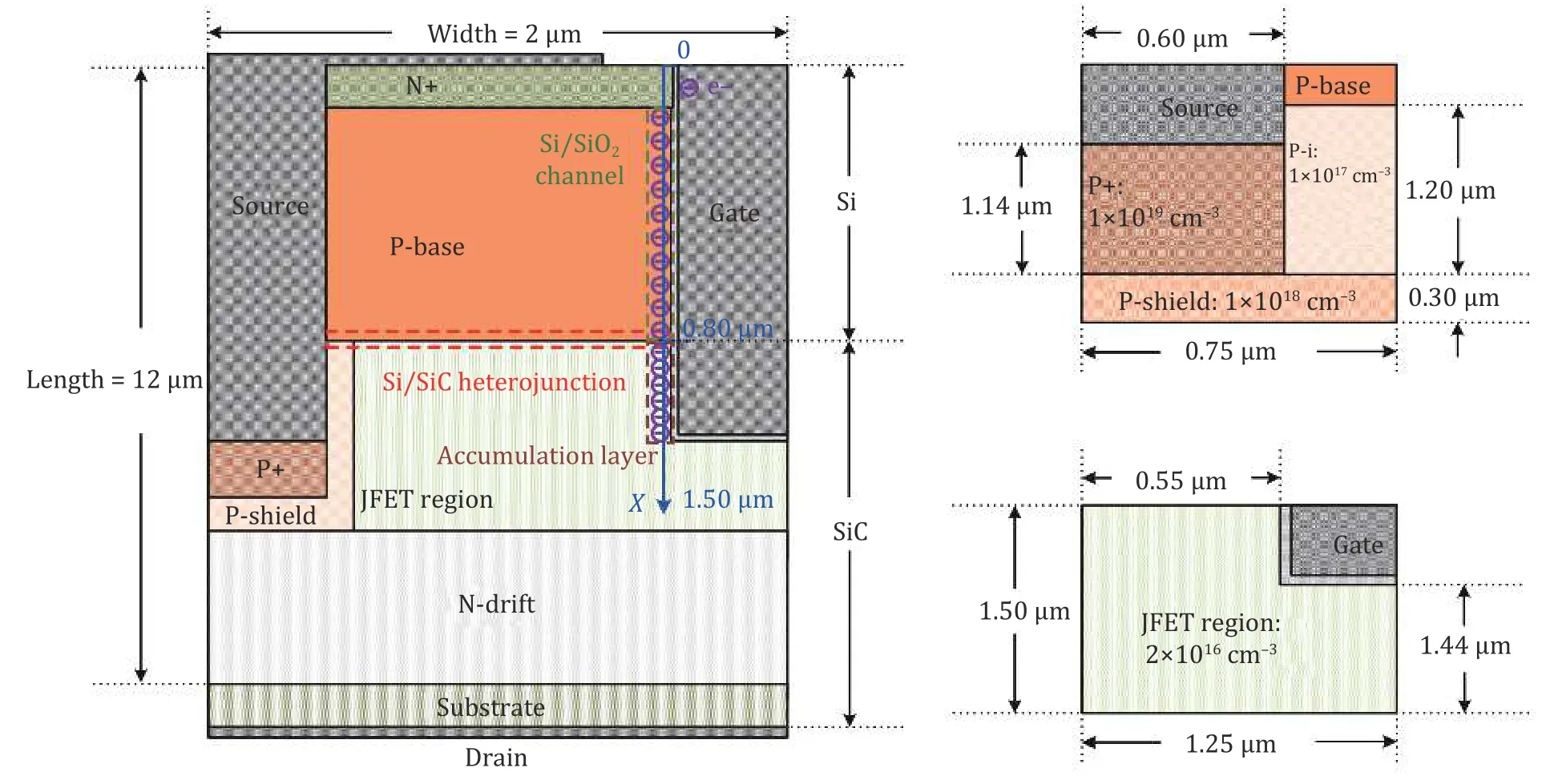
Fig.1.Schematic illustration of the device structure and the structure parameters of the P-shield and JFET regions.The P-base and N+ regions are made of Si.The JFET,P-shield,N-drift,and substrate regions are made of SiC.In contrast,DT-MOS is made of pure SiC.The regions marked with electrons are the inversion layer (IL) and AL.The arrow of the X axis extends from IL to the JFET region.
The channel mobility of DT-MOS was set to 20 cm2/V·s.The standard band-to-band tunneling(BBT-STD) model and the trap-assisted tunneling(TRAP.TUNNEL) model in the Silvaco TCAD tool is utilized to simulate the tunneling effect in the HDT-MOS structure.The parameters in the models are set to be defaults in the Silvaco tool.
2.2 Gate-controlled tunneling mechanism
We considerVGin HDT-MOS to influence the heterojunction current characteristics,which we call the gate-controlled tunneling effect.In this effect,a high tunneling current is obtained under the control ofVG,and the current is determined byVG.A positiveVGvalue can control the surface potential and has two effects on the semiconductor: Inversion and accumulation.In HDT-MOS,the inversion effect changes the conductivity type of Si in the heterojunction,and the accumulation effect can increase the carrier concentration of SiC.In HDT-MOS,the heterojunction is pN-type (formed with a p-type narrow bandgap semiconductor and an N-type wide bandgap semiconductor) without the gate bias voltage.However,the pN-type heterojunction near the gate oxide transforms into an nN-type heterojunction (formed with an n-type narrow bandgap semiconductor and an N-type wide bandgap semiconductor) with the effect of positiveVGdue to channel inversion.The energy band shown in Fig.2 (a) is the transformed nN-type heterojunction in HDT-MOS without AL.There occurs a band offset in the heterointerface that results in a high interface barrier similar to the Schottky barrier.The nN-type heterojunction also exhibits a rectification behavior.A positive drain-to-source voltage (VD) puts a reverse bias on the heterojunction in HDT-MOS,and the high reverse resistance of the heterojunction leads to the degeneration of the forward characteristics of HDT-MOS.
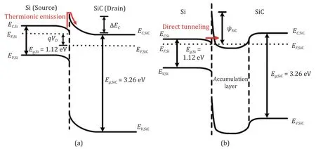
Fig.2.Energy band schematic diagrams of (a) nN-type heterojunction with high potential on the SiC side and (b) nN-type heterojunction with IL and AL in HDT-MOS.
The main transport mode for electrons in the condition of Fig.2 (a) is the thermionic emission mode,which means that few electrons can transfer through the barrier.However,the electrons can also transfer by direct tunneling,and the tunneling probability (Pt) is determined by the distance that electrons need to tunnel through.If the width of the barrier decreases to a small value,the main transport mode for electrons will change to the direct tunneling mode due to the increase in the tunneling current.In this condition,a larger current can be achieved.
In HDT-MOS,a narrow heterointerface barrier for direct tunneling of electrons is obtained owing to the accumulation effect of positiveVG,as shown in Fig.2 (b).Since the trench gate extends into SiC JFET,AL forms with positiveVG,and the energy level in AL reduces.With the increase in positiveVG,the carrier concentration in AL increases,resulting in a lower energy level.The higher carrier concentration leads to a much smaller width of the barrier region in the nN-type heterojunction.Thus,when in on state,the heterojunction in HDT-MOS exhibits an Ohmic behavior,and the value of the tunneling current is controlled byVG.Referring to the Ohmic contact resistance,the tunneling current of the nN-type heterojunction (IHT) can be analyzed by a simplified formula:
whereψSiCis the heterointerface barrier height,nALis the concentration of electrons in AL,is the electron effective mass,is the Planck constant,ε0is the permittivity of vacuum,andεris the relative permittivity of SiC.
SinceψSiCis not sensitive to the variations innAL,andIHTis highly positively correlated withnAL.According to the Fermi-Dirac distribution,nALcan be evaluated with the formula:
whereNcis the density of the effective states in the conduction band,kis the Boltzmann constant,Tis the absolute temperature,EFis the Fermi level,is the conduction level without the surface potential,VFBis the flat band voltage,Voxis the voltage on the gate oxide,andF1/2(x) is the Fermi-Dirac integral which increases rapidly with increasingx.Some core parameters of SiC and Si materials are list in Table 2.Under the control of positiveVG,the energy level at the semiconductor surface decreases,as shown in Fig.2.Therefore,nALis controlled byVG,and a higherVGvalue leads to a highernALvalue.Consequently,the gate-controlled tunneling effect leads to a highIHTvalue in HDT-MOS,and the value ofIHTis controlled byVG.
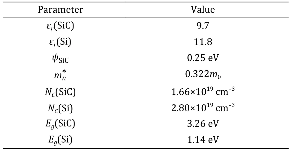
Table 2 Core parameters.
The analysis of the gate-controlled tunneling effect in HDT-MOS has been demonstrated through simulations,and the results are shown in Fig.3 (a).With the increase inVG,the energy level on the Si side of the heterointerface declines,which manifests IL formed,and the pN-type heterojunction transforms into the nN-type when in on state.The energy level drops on the SiC side of the heterointerface (in AL),thereby decreasing the width of the heterointerface barrier.Thus,both a high tunneling current and a low interface resistance are achieved at the heterojunction in HDT-MOS.A higherVGvalue results in a higher carrier concentration,a lower energy level in AL,a narrower heterointerface barrier,and a higher tunneling current.

Fig.3.Simulation results for EC of the heterojunction with (a) different VG and WAL=0.06 μm (Ec near the interface is shown in the dashed frame) and (b) different WAL and VG=15 V; in the direction of the arrow,WAL is 0,0.01 μm,0.02 μm,0.03 μm,0.04 μm,0.05 μm,0.06 μm,0.07 μm,0.08 μm,0.09 μm,0.10 μm,and 0.20 μm.The region corresponding to the X axis is indicated in Fig.1.
Fig.3 (b) shows the influence of theWALvalue on the heterojunction energy band atVG=15 V.WhenWALis small,AL cannot form a high electron concentration region completely,and theVGcontrol of the energy level is weak.Consequently,most of the electrons cannot tunnel through the interface barrier because of highECon the SiC side.AsWALincreases,the energy level dips on the SiC side of the heterointerface,and the heterointerface barrier becomes steep and narrow,making it easy for electrons to tunnel through the heterojunction barrier.
2.3 Heterointerface traps and charges analysis
The dislocation states at the heterointerface can influence theI-VandC-Vcharacteristics of the heterojunction [19].It has been demonstrated that the heterointerface states increase the leakage current of the heterojunction [20].The increase in the leakage current that we consider is caused by trap-assisted tunneling.The trap states provide a defect energy level in the heterointerface barrier and lead to trap-assisted tunneling of electrons,as shown in Fig.4 (a).The electrons tunnel into the defect energy level before transferring into SiC,resulting in a much smaller electron tunneling distance and higher tunneling current.
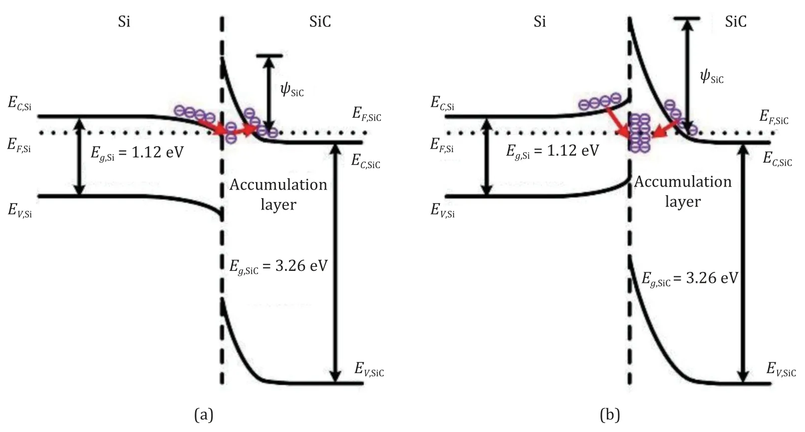
Fig.4.Schematic diagrams of the nN-type heterojunction energy bands with (a) trap-assisted tunneling effect in HDT-MOS and (b) extremely high interface state density.
Some studies have investigated the influence of heterointerface states by simulations with the donor-type heterointerface charge (electron) [21,22].We consider that the donor-type heterointerface charge can reduce the tunneling distance for electrons similarly to trap-assisted tunneling.Therefore,the donor-like heterointerface charge can significantly increase the forward current of HDT-MOS.The heterointerface charge defaults to the donor type in the rest of the paper.
For the condition of interface states with a deep energy level and a much higher density,most of the nearby electrons are captured by the states to cause Fermi energy level pinning.The flat band voltage of the heterojunction increases with increasing interface states.Thus,with an extremely high interface state density,a much higher and wider heterointerface barrier is formed in HDT-MOS,as shown in Fig.4 (b),and the forward current decreases dramatically.Therefore,the donor-like traps are introduced into HDT-MOS for this condition.The heterointerface charge also leads to a higher gate charge for HDT-MOS.Consequently,worse dynamic performance is obtained by HDT-MOS with the increase of the heterointerface charge.
3 Simulation results and discussion
3.1 Optimization of structure parameters
The P-shield region can suppress the electric field in both the gate oxide and heterointerface,while the protruded gate oxide can also shield the Si/4H-SiC heterointerface.Thus,WALhas an influence on the electric field at the gate oxide and heterointerface,as shown in Fig.5 (a).The shallower depth of trench gate oxide leads to a lower maximum electric field of the gate oxide (Eox-m) but increases the maximum electric field of the Si region (ESi-m) whenWALdecreases.As the electric field contours of HDT-MOS with four different conditions shown in Figs.5 (b)–(e),the P-shield region shows a great shield effect on the electric field of the gate oxide.Even ifWALis set to be 0.2 μm,Eox-mof HDT-MOS still stays below 2.2 MV/cm atVD=1200 V.

Fig.5.Influence of WAL on the reverse electric field of HDT-MOS: (a) tradeoffs between Eox-m and ESi-m with varying WAL for HDT-MOS; electric field contours with (b) WAL=0.06 μm and VD=1200 V,(c) WAL=0.06 μm and VD=1700 V,(d) WAL=0.20 μm and VD=1200 V,and (e) WAL=0.20 μm and VD=1700 V.Dox is the distance to the oxide at the Si surface of the heterointerface.
ESi-mcan be decreased by the increase ofWALin HDT-MOS,and the electric field distribution curves of the Si surface of the Si/4H-SiC heterointerface with differentWALare shown in Figs.6 (a) and (b).With largerWAL,ESi-mis significantly decreased and the highest electric field point is transferred from the SiC/SiO2interface to the middle of the Si surface due to the shield effect of the trench gate oxide.
Fig.6 (c) shows the electric field distribution curves which are perpendicular to the heterointerface at the highest electric field point of HDT-MOS withWAL=0.06 μm andWAL=0.20 μm,respectively.There occurs a field offset in the heterointerface,which we consider is attributed to the permittivity difference between Si and 4H-SiC (11.9 and 9.7,respectively).WithWAL=0.20 μm,ESi-mof HDT-MOS is 0.292 MV/cm atVD=1700 V and the Si region is greatly shielded from the high electric field.With the optimizedWALvalue of 0.06 μm,the higherESi-mvalues of 0.417 MV/cm and 0.503 MV/cm are obtained by HDT-MOS withVD=1200 V andVD=1700 V,respectively.However,the breakdown region of HDT-MOS is still the P-shield region in this condition owing to the high doping concentration of the Si P-base region (4×1017cm–3).According to the condition of avalanche breakdown,the critical electric field of N-type Si under the avalanche breakdown state(EN-Si) can be evaluated by the formula [23]:
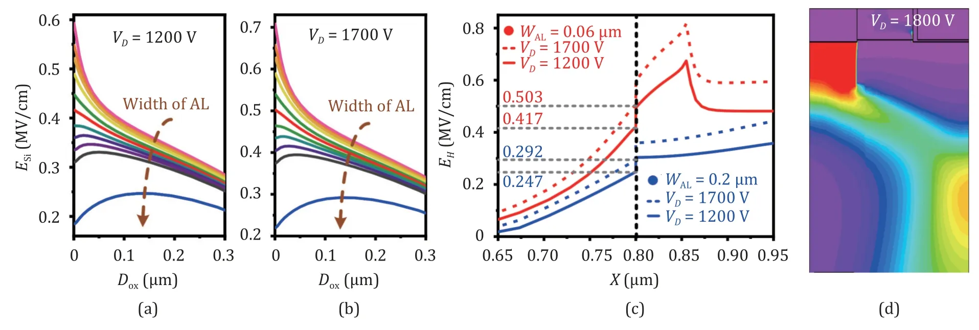
Fig.6.Inflence of WAL on the electric field of the heterojunction in HDT-MOS.Electric field distribution curves of the Si surface of the heterointerface with different WAL at (a) VD=1200 V and (b) VD=1700 V.In the arrow direction in (a) and (b),WAL is 0,0.01 μm,0.02 μm,0.03 μm,0.04 μm,0.05 μm,0.06 μm,0.07 μm,0.08 μm,0.09 μm,0.10 μm,and 0.20 μm.The region corresponding to the Dox axis is indicated in Fig.5 (b).(c) Electric field distribution curves of the heterointerface (EH)at the highest electric field point in HDT-MOS.The region corresponding to the X axis is indicated in Figs.5 (b) and (d).(d) Current distribution of the HDT-MOS structure after breakdown (VD=1800 V).
whereNDis the concentration of the donors.WhenND=4×1017cm–3,theEN-Sivalue of 0.636 MV/cm is obtained.In Si materials,the collisional ionization coefficient of electrons is higher than that of holes [24],resulting in a higher critical electric field for P-type Si under the avalanche breakdown state.Thus,the critical electric field for the Si P-base region with the doping concentration of 4×1017cm–3is higher than 0.636 MV/cm and the Si region in HDT-MOS is not broken down withESi-m=0.503 MV/cm shown in Fig.6 (c).It can be demonstrated by the current distribution of HDT-MOS after breakdown,and the breakdown point occurs at the corner of the P-shield region,as shown in Fig.6 (d).
TheWALvalue also affectsRON-SPand the switching loss,as shown in Fig.7 (a).ForWALless than 0.05 μm,the gate-controlled tunneling effect does not work,andRON-SPof HDT-MOS increases rapidly with decreasingWALdue to the high heterointerface barrier.A decrease inWALleads to the lower MOS capacitance between the gate and drain and results in a lower switching loss.For these two structures,WAL=0.06 μm is chosen as the optimized value for further study throughout the rest of this paper.
The smaller number of interface states and the narrower bandgap lead to lowerVTHfor HDT-MOS with the same P-base doping concentration compared with that of DT-MOS,thereby decreasing the gate drive voltage and consequently enhancing the reliability of the gate oxide in potential applications.VTHandRON-SPincrease with increasing the P-base doping concentration (NP-base),as shown in Fig.7 (b).Therefore,HDT-MOS withNP-base=4×1017cm–3can obtain a similarVTHvalue compared with that of DT-MOS withNP-base=1×1017cm–3,as shown in the inset transfer characteristic curves in Fig.7 (b).TheNP-baseconcentration values of 4×1017cm–3and 1×1017cm–3were chosen for HDT-MOS and DT-MOS,respectively,to perform comparative studies of these two structures with similarVTH.
With the constant value ofWP-base,WP-shieldwill influence the forward and reverse performance of HDT-MOS simultaneously,as shown in Fig.7 (c).RON-SPincreases with the increase ofWP-shielddue to the increase ofRJ.Eox-mreduces and BV increases whileWP-shieldincreases owing to the smaller distance between two adjacent P-shield regions.It should be noted that BV will degenerate suddenly whenWP-shieldis smaller than 0.75 μm due to the punch-through effect.As a result,theWP-shieldvalue of 0.75 μm is chosen for HDT-MOS and DT-MOS.
3.2 Device characteristics and analysis
Compared with DT-MOS,the proposed HDT-MOS achieves lowerRON-SPwith similar BV,as shown in Fig.8 (a).Fig.8 (b) analyzesRON-SPof these two devices where the estimation values are given.RON-SPconsists of five components: The source resistanceRS,the channel resistanceRCH,the heterointerface resistanceRH,RJ,and the drain resistanceRD.RS,RJ,andRDare essentially identical for these two structures; the main difference in totalRON-SPoriginates fromRHandRCH.There is noRHin DT-MOS,while the magnitude ofRHin HDT-MOS is significantly reduced due to the gate-controlled tunneling effect.The channel in HDT-MOS exhibits much higher mobility and a higher carrier density than DT-MOS owing to the smaller number of interface states and smaller bandgap of Si.Thus,RCHof HDT-MOS is much lower than that of DT-MOS,and lowerRON-SPis obtained by HDT-MOS.
The gate charges of the devices were evaluated with the test circuit shown in the inset of Fig.8 (c).The gate platform voltage (VGP) of HDT-MOS is lower than that of DT-MOS.VGPcan be expressed by
whereJON-SPis the on-state current density,WCellis the cell width,LCHis the channel length,μCHis the channel mobility,andCoxis the oxide capacitance.AsμCHof HDT-MOS is much higher than that of DT-MOS,HDT-MOS exhibits lowerVGP.The Miller capacitance (Crss) of HDT-MOS is lower than that of DT-MOS due to the change in the P-base region,andCrssincreases asVGincreases; thus,this lowerVGPof HDT-MOS corresponds to much lowerCrsswhenVG=VGP.Theoretically,VGis invariant during the gate voltage platform,andQGDdepends solely onCrss.Nevertheless,VGalways rises during the opening period in the actual test.TheVGvalues of the two structures increase slowly during the gate voltage platform,and the variation value inVGP(ΔVGP) of HDT-MOS is much lower than that of DT-MOS.We attribute the lower ΔVGPof HDT-MOS to the narrower bandgap and the higher carrier mobility of the Si channel.The narrower bandgap and the higher carrier mobility lead to much lowerRCHof HDT-MOS and result in a much lower voltage drop on the channel than that of DT-MOS with the similar forward current,which means that the channel pinch-off is much slighter for HDT-MOS during the gate voltage platform.Besides,the higher concentration of the Si channel carriers caused by the narrower bandgap can weaken the short channel effect.Therefore,the significantly lower ΔVGPis obtained by HDT-MOS.The lower ΔVGPleads to fewer extra charges to the gate-to-source capacitance (CGS)during the gate voltage platform and results in a shorter gate voltage platform,namely,lowerQGD.Therefore,QGDis 52.59% lower in HDT-MOS than that in DT-MOS.However,QGof HDT-MOS is higher than that of DT-MOS owing to lowerVGPand higherCGS.
The switching performance of the HDT-MOS and DT-MOS devices is compared in Fig.9.The switching loss of HDT-MOS is significantly lower than that of DT-MOS because of lowerQGDandRON-SPof HDT-MOS.In the switching tests,a higher potential difference betweenVGandVGPresults in a higher gate current and a shorter switching time.Because of the higher potential difference betweenVGandVGP,the turn-on time (TON) is much shorter than the turn-off time (TOFF) for both structures.A comparison of the main characteristics of HDT-MOS and DT-MOS is listed in Table 3 and the measure conditions of some parameters areVG=15 V andVD=1 V forRON-SP;IDS=100 mA/cm2forVTH;VD=1200 V forEox-m;VD=800 V and Frequency=1 MHz for the Miller capacitanceCrss; the heterointerface charge concentrationQI=0 in HDT-MOS.All the measure conditions are similar to the commercial product conditions exceptRON-SP.In this work,RON-SPis measured at the condition ofVG=15 V andVD=1 V,while the commercial product condition isVG=20 V andIDS=IRated,whereIRatedis the rated current.HigherVGcan decreaseRON-SPfor both HDT-MOS and DT-MOS,and whetherVGis 15 V or 20 V,the advantages ofRON-SPof HDT-MOS are similar.Without the actual package and area,the simulated devices cannot setIRated,thus we choseVD=1 V to be the measure condition ofRON-SP.

Fig.9.Transient switching behavior and switching loss with the test circuit shown in the inset.The device area and gate resistance RG were set as 1 cm2 and 5 Ω,respectively.The driving signal of the gate was switched between –5 V and 15 V.The TON values of 57 ns and 78 ns and TOFF values of 39 ns and 46 ns were obtained for HDT-MOS and DT-MOS,respectively.
The temperature has a significant influence on the performance of the power device.For the HDT-MOS device,the temperature will greatly affect the leakage current (IDSS),as shown in Fig.10.IDSSincreases with the temperature rise,and it increases much faster when the temperature exceeds 400 K.IDSSincreases to a non-negligible value when the temperature exceeds 400 K,leading to a significant reduction of BV.Besides,the thermal expansivity of Si and SiC is different,which may lead to a thermal mismatch for HDT-MOS at high temperatures.Therefore,after the long-time power cycling,IDSSof HDT-MOS may further increase.

Fig.10.Influence of the temperature on BV and IDSS.
3.3 Influence of heterointerface traps and charges
Fig.11 (a) shows theI-Vcharacteristic curves of HDT-MOS for differentQIvalues.With increasingQI,the forward current increases,andRON-SPdecreases owing to the decrease inRHcaused by trap-assisted tunneling.TheRON-SPvalues of 3.24 mΩ·cm2,3.06 mΩ·cm2,2.62 mΩ·cm2,and 2.28 mΩ·cm2are obtained forQI=0,QI=2.3×1011cm–3,QI=1.0×1012cm–3,andQI=2.3×1012cm–3in HDT-MOS,respectively.
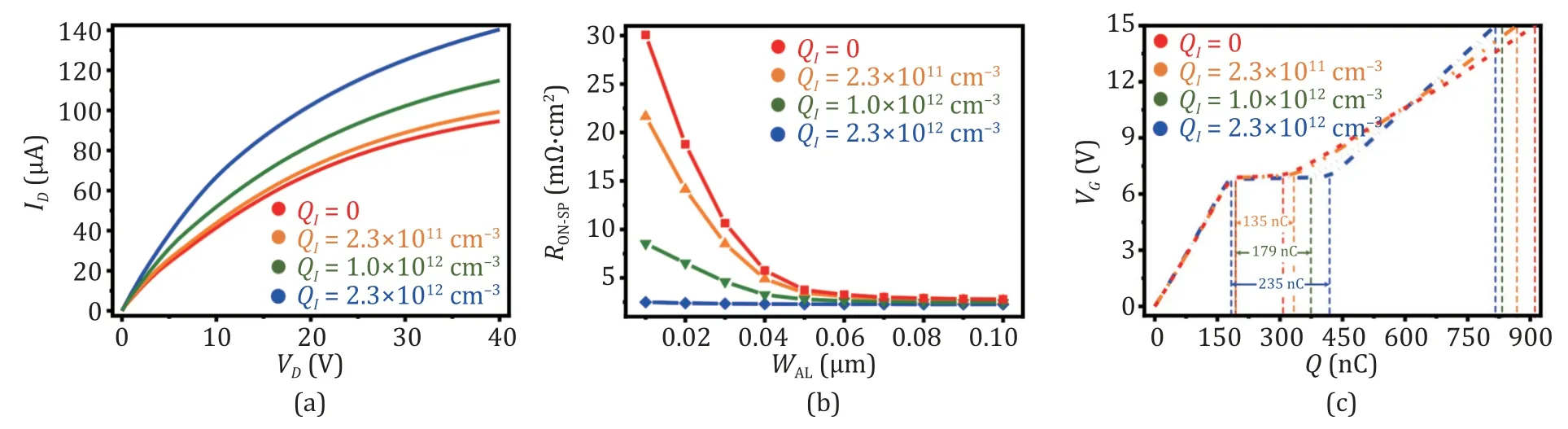
Fig.11.Influence of QI on the performance of the HDT-MOS structure: (a) output I-V characteristic curves of HDT-MOS for different QI,(b) influence of WAL on RON-SP of HDT-MOS for different QI,and (c) gate charge tests of HDT-MOS for different QI.The area of each device was set to 1 cm2.The QGD values of 135 nC/cm2,179 nC/cm2,and 235 nC/cm2 and the QG values of 865 nC/cm2,838 nC/cm2,and 817 nC/cm2 were obtained for the HDT-MOS device when QI=2.3×1011 cm–3,QI=1.0×1012 cm–3,and QI=2.3×1012 cm–3,respectively.
A higherQIvalue in HDT-MOS leads to a lower influence ofWALonRON-SP,as shown in Fig.11 (b),and this effect is attributed to the decrease inRHwith increasingQI.TheRON-SPvalue of HDT-MOS sharply increases with smallWALwhenQI=0 due to the increasedRHvalue.However,RHcan be significantly reduced with the influence of highQI,resulting in the decrease inRON-SPof HDT-MOS with smallWAL.WALhas little effect onRON-SPof HDT-MOS whenQIis greater than 2.3×1012cm–3.
In HDT-MOS,QGDincreases with increasingQI,whileQGdecreases,as shown in Fig.11 (c).QIcauses the extra charges forQGDand increasesCGD,resulting in higherQGDin HDT-MOS.The influence of the heterointerface traps can also significantly affect the forward performance of HDT-MOS.The influence of acceptor-like traps is similar toQIso that we only show the influence of donor-like traps in Fig.12.The increase in the density of the donor-like hetereinterface traps (DHit-donor) leads to the degeneration ofRON-SPof HDT-MOS.TheRON-SPvalues of 3.32 mΩ·cm2,3.50 mΩ·cm2,and 3.82 mΩ·cm2are obtained forDHit-donorof 5×1012cm–3,1×1013cm–3,and 5×1013cm–3in HDT-MOS,respectively.
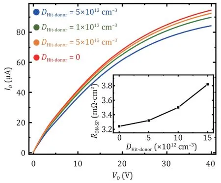
Fig.12.Output I-V characteristic curves of HDT-MOS for different DHit-donor.
4 Conclusions
The HDT-MOS structure,which features the high channel mobility and low working loss,and the gate-controlled tunneling effect are proposed.The proposed HDT-MOS is demonstrated to possess the advantages of both Si and SiC,namely,high channel mobility and high critical electric field,respectively.The gate-controlled tunneling effect demonstrates that the AL electron concentration increases with increasingVG,and the higher AL electron concentration reduces the level of the energy band on the SiC side of the heterointerface,creating a narrower interface barrier through which electrons can easily tunnel,thereby decreasingRH.The heterointerface charges positively influence the forward current with the trap-assisted tunneling effect while increasingQGDof HDT-MOS.Oppositely,the donor-like heterointerface traps will increaseRON-SP.Consequently,a lowRON-SPvalue and a high BV value are simultaneously achieved in HDT-MOS.TheRON-SP,QGD,switching loss,andQGD×RON-SPvalues of HDT-MOS are 19.21%,52.14%,22.59%,and 61.25% lower,respectively,than those of the corresponding DT-MOS structure.As the results,the significantly lower working loss is obtained by HDT-MOS and the temperature rise of the device working as a power switch can be greatly suppressed.
Funding
This work was supported by the Major Science and Technology Program of Anhui Province under Grant No.2020b05050007.
Declaration of competing interest
The authors declare no conflicts of interest.
 Journal of Electronic Science and Technology2023年4期
- Journal of Electronic Science and Technology的其它文章
- Developing microwave-induced thermoacoustic tomography: System,application,and reconstruction
- Life-cycle assessment of batteries for peak demand reduction
- High-sensitivity phase imaging eddy current magneto-optical system for carbon fiber reinforced polymers detection
- Algorithms for automatic measurement of SIS-type hysteretic underdamped Josephson junction’s parameters by current-voltage characteristics
- Boundedness and liveness enforcement for labeled Petri nets using transition priority
- Characteristics of sub-synchronous oscillation in grid-connected wind farm system