
Electronic structures and topological properties of TeSe2 monolayers*
2021-11-23 07:30ZhengyangWan萬正陽HaoHuan郇昊HairuiBao鮑海瑞XiaojuanLiu劉曉娟andZhongqinYang楊中芹
Chinese Physics B 2021年11期
Zhengyang Wan(萬正陽) Hao Huan(郇昊) Hairui Bao(鮑海瑞)Xiaojuan Liu(劉曉娟) and Zhongqin Yang(楊中芹)
1State Key Laboratory of Surface Physics and Key Laboratory of Computational Physical Sciences(MOE)&Department of Physics,Fudan University,Shanghai 200433,China
2Collaborative Innovation Center of Advanced Microstructures,Nanjing 210093,China
Keywords: two-dimensional material,monolayer TeSe2,quantum spin Hall effect,topological insulator
1. Introduction
Since the discovery and successful fabrication of graphene,[1]two-dimensional(2D)materials have attached intensive attention because of their many novel physical properties, such as the quantum spin Hall (QSH) effect,[2]quantum anomalous Hall (QAH) effect,[3]valley Hall effect,[4]etc,making them be promising candidate materials for future high performance electronic, spintronic, and optoelectronic devices.[4-7]Currently,besides graphene,[8,9]various types of 2D materials have also been synthesized in experiments, including elemental 2D films from group III to group V, such as boronene,[10-12]silicene,[13-15]stanine,[16]black phosphorus films,[17-19]antimonene,[20,21]and bismuthine.[22]Some binary 2D compounds such as MoS2[23-26]and CrI3[27]and so on were also fabricated successfully. Although plenty of 2D materials were reported owning QSH or QAH effects,[2,28,29]only few systems having the QSH(such as the HgTe/CdTe[30]quantum well and bismuthine[22])or QAH(such as Cr doped(Bi,Sb)2Te3film[31])effects were confirmed in experiments.
Based on previous developments, researchers have extended the 2D materials to group-VI monolayers.In 2017,Zhuet al.[32]studied the structures and stability of tellurene (2D Te monolayers)using the particle-swarm optimization method in combination with density functional theory. And bilayer tellurene films have been observed in their experiments.[32]Different from two atomic layers in silicene and black phosphorus monolayers, tellurene contains trilayers,[32]with the central-layer Te behaving metal-like and the two outer layers semiconductor-like. They found that this unique multivalent behavior of Te guarantees the structural stability of the material.[32]Yanet al.found two ultra-stable novel allotropes for Te few-layers from first-principles calculations.[33]These studies promoted the researches on the group-VI monolayer materials. It is meaningful to explore the electronic structures and the interesting topological effects in group-VI monolayer materials.
In this work, the electronic structures and topological properties of a group-VI binary compound of TeSe2monolayers are studied based on the density functional theory and Wannier function method. Three types of structures, namely,α-TeSe2,β-TeSe2,andγ-TeSe2,are proposed and studied,all of which are semiconductors with indirect band gaps. Theγ-TeSe2monolayer is found being a QSH insulator with a global nontrivial energy gap of 0.14 eV when a 3.5% compressive strain is applied. The topology of the material is identified by the calculations ofZ2topological invariants and the edge state. The opening mechanism of the global nontrivial band gap is analyzed.
2. Computational models and methods
For the 2D trilayered tellurene, the multiple valences of Te atoms promote the formation of a stable monolayer tellurene structure. Based on the studied structures of tellurene[32]and tellurium few-layers,[33]we build and consider three typical structures for the TeSe2monolayers. To obtain the TeSe2, the Te atoms in the two outer layers of tellurene are all replaced by Se atoms. Since Se electronegativity is larger than that of Te,the TeSe2structures are expected to be also very stable. The built three type structures for the TeSe2monolayers, namedα,β, andγphases, are illustrated in Figs. 1(a)-1(c), respectively. Theα-TeSe2has a similar structure to that of 1T-MoS2.[34]Both the Se1 and Se2,corresponding to the S atoms in the 1T-MoS2,are in the outer layers of the materials, with the coordination number of 3. The central-layer Te atoms correspond to the Mo atoms in the 1TMoS2,with the coordination number of 6. For theβ-TeSe2,it presents a corrugated structure. In the top view, the structure is composed of hexagons and rhombuses. The coordination number of each Te atom in theβ-TeSe2is 4,different from that in theα-TeSe2. Theγ-TeSe2has a similar geometric structure to that of 2H-MoS2,[34]with an in-plane mirror symmetry.Exotic properties may be dug out from these various structures of the TeSe2monolayers.
The electronic states of the TeSe2monolayers with the three type structures are calculated within the framework of density functional theory (DFT), as implemented in the Viennaab initiosimulation package (VASP).[35]The projected augmented wave(PAW)potentials are adopted to deal with the electron-ion interactions.[36,37]The Perdew-Burke-Ernzerhof generalized gradient approximation (GGA-PBE) is used for the exchange-correlation functional.[38]A vacuum layer of 20 ?A is applied between the neighboring TeSe2layers to minimize the image interactions from the periodic boundary condition. The plane wave cutoff energy is set to be 500 eV.TheΓcenteredk-point sampling of 15×15×1 is adopted in the first Brillouin zone. The structures are optimized until the force on each atom is less than 0.01 eV/?A.To investigate the dynamic stability of the proposed TeSe2ML,phonon dispersion is calculated by using the DFT perturbation theory as implemented in the PHONOPY code. TheZ2topological invariant is calculated with the maximally localized Wannier functions[39]by using the Wannier 90 package. To obtain the edge states, we construct a TB Hamiltonian with a basis of maximally localized Wannier functions by using the Wannier Tools[40]package.
3. Results and discussion
3.1. Structures and electronic states of the TeSe2 monolayers
We now study the geometric structures and the electronic states of the TeSe2monolayers with the three type structures(Figs.1(a)-1(c)). The optimized structural parameters and the calculated cohesive energies of the three materials are listed in Table 1. The bond lengths of the neighboring Te and Se atoms(2.82-2.87 ?A) are close to each other for the three structures studied. Due to the largest area of the 2D unit cell inβ-TeSe2,the layer thickness(dz)inβ-TeSe2is the smallest,corresponding to the smallest angle(θ)between the Te-Se bond and the horizontal direction (Table 1). Inγ-TeSe2, the Se1 is exactly localized on the top of the Se2.The strong repulsive forces between the two type anions (Se1 and Se2) result in the largest layer thickness in the structure,as seen from Table 1. Among the three structures,α-TeSe2has the largest cohesive energy whileγ-TeSe2has the smallest one.Thus,α-TeSe2is the most stable structure and the other two structures are metastable.The first Brillouin zones ofα-TeSe2(γ-TeSe2) andβ-TeSe2are hexagon and rectangle,respectively(Fig.1(d)).
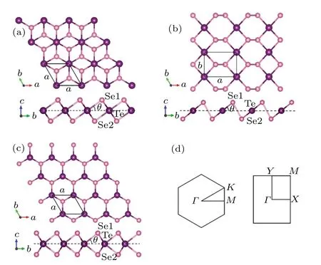
Fig.1. Top and side views of the optimized structures of α-TeSe2 (a),β-TeSe2 (b),and γ-TeSe2 (c). (d)The first Brillouin zones of α-TeSe2 or γ-TeSe2 (left)and β-TeSe2 (right).
The calculated band structures ofα-TeSe2,β-TeSe2,andγ-TeSe2are displayed in Figs. 2(a)-2(c), respectively. The Fermi level(EF)is set at energy zero. The red dotted and the black solid curves present the bands for the materials without and with spin-orbit coupling(SOC)interactions,respectively.The SOC interactions do not change much the bands on the whole but can split the energy degeneracy at some positions in the momentum space, such as the places marked by the green ovals in Figs.2(a)and 2(c). The three materials are all semiconductors with indirect band gaps.The SOC interactions slightly reduce the band gaps due to the energy splitting. The energy bands ofα-TeSe2andβ-TeSe2with SOC are both doubly degenerate, while the bands ofγ-TeSe2are not. The reason is that both time-reversal and space-inversion symmetries are owned by theα-TeSe2andβ-TeSe2monolayers, while there is no space-inversion symmetry in theγ-TeSe2monolayer(Fig.1). In Figs.2(a)-2(c),three group bands are clearly observed in the band structures ofα-TeSe2andγ-TeSe2. This similarity can be ascribed to the relatively similar structures of the two materials(Figs.1(a)and 1(c)).
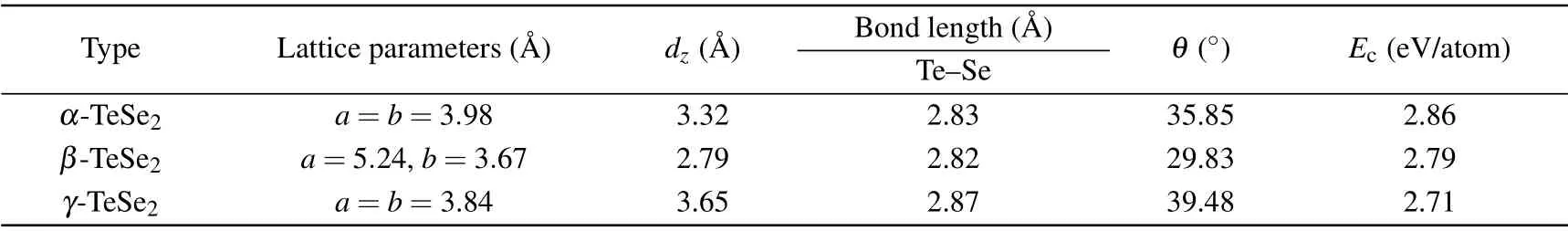
Table 1. The results for the monolayer TeSe2 with different structures. The properties listed contain the lattice constants a and b,distance between the upper and lower Se atomic layers(dz),Te-Se bond length,angle between the Te-Se bonding direction and the horizontal direction(θ,marked in Fig.1),and the cohesive energy(Ec).
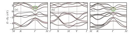
Fig.2. Band structures of α-TeSe2 (a),β-TeSe2 (b),and γ-TeSe2 (c)without(red dotted curves)and with(black solid curves)the consideration of SOC.
The similar structures ofα-TeSe2andγ-TeSe2also give rise to the close band gaps of the two materials (Fig. 3(a)).When the SOC is turned on,the band gaps ofα-TeSe2andγ-TeSe2are 0.38 eV and 0.65 eV, respectively. The obtained energy bands ofβ-TeSe2are given in Fig. 2(b), which are consistent with the results reported in Ref. [41]. The largest band gaps achieved inβ-TeSe2(Fig.3(a))can be ascribed to the relatively flat bands localized at the valence-band top and conduction-band bottom in the material(Fig.2(b)). The analysis of the orbital-resolved bands(not shown)shows that these flat bands are primarily composed of the pzorbitals of the Se1 and Se2 atoms. Thus,the dangling bonds of the Se pzorbitals in the uniqueβ-TeSe2structure cause the relatively large band gaps in the materials.
Forα-TeSe2(γ-TeSe2), before the SOC is taken into account, doubly degenerate bands around 1.3 eV (1.0 eV)marked by green ovals occur, composed mainly by pxand pyorbitals of the Te and Se atoms (to be discussed), due to theC3vsymmetry in the monolayers. This degeneracy is lifted after the SOC is turned on. A pretty large direct band gap of 0.4/0.7 eV is opened there by the SOC in theα-TeSe2/γ-TeSe2monolayer due to the stronger intrinsic SOC coming from the pxand pyorbitals,compared to that from the pzorbitals.[42,43]The gaps opened in such kind of parabolic bands are generally topologically nontrivial, leading to the appearing of the QSH[44]or QAH[45,46]insulators with a non-Dirac-type bandgap opening mechanism. Since the concerned band gaps inαTeSe2andγ-TeSe2are nonglobal,the materials are in topological semimetal states. As displayed in Fig. 2(a), the dispersion of the bands around 1.3 eV ofα-TeSe2is very large.Expectably,it is difficult to tune the bands to produce a global topologically nontrivial band gap in theα-TeSe2monolayer.Therefore,theγ-TeSe2monolayer is focused in the following.

Fig.3. (a)The band gaps of the three materials studied. The rectangles without and with the grids give the band gaps without and with the consideration of SOC.(b)The phonon spectrum of the γ-TeSe2 monolayer.
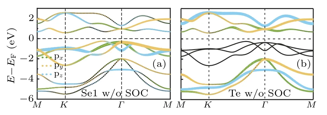
Fig. 4. The energy band projection of the Se1 (a) and Te (b) atoms in the γ-TeSe2 monolayer without the consideration of SOC. The green,yellow,and blue colors represent the contributions from the px,py,and pz orbitals of the corresponding atom,respectively.
In terms of the stability of theγ-TeSe2structure, the phonon spectrum is calculated and shown in Fig. 3(b). No negative frequency is found in Fig. 3(b), indicating the dynamic stability of theγ-TeSe2despite its lowest cohesive energy among the three structures. To deeply understand the electronic structure ofγ-TeSe2, the projected band structures of the Se1 and Te atoms are plotted in Fig.4 without considering SOC. Due to the in-plane mirror symmetry owned byγ-TeSe2(withD3hspace group), the upper layer Se1 and the lower layer Se2 atoms are equivalent.Therefore,only the band projection of the Se1 atom is analyzed. As shown in Figs.4(a)and 4(b),the valence-band top and conduction-band bottom at theΓpoint, with double degeneracy, are mainly contributed by the pxand pyorbitals of the Te or Se atoms. The degeneracy is lifted after the SOC is turned on. From the orbital distribution of the Se1 and Te atoms (Fig. 4), we can clearly find the bonding,nonbonding,and antibonding characteristics between the Se and Te atoms. The bonding states are formed between?6 eV and?2 eV.The nonbonding states are formed between?2 eV and 0 eV and antibonding states are formed between 0.5 eV and 2.8 eV.
3.2. Strain effects in γ-TeSe2
As an effective means to tune electronic structures,strain has been applied in multiple material systems.[47-50]We here apply in-plane biaxial strain to theγ-TeSe2monolayer,which is defined asε=(a?a0)/a0,wherea(a0)is the strained(unstrained) in-plane lattice constant. The positive and negative values ofεcorrespond to the tensile and compressive biaxial strains,respectively. The band evolution ofγ-TeSe2under different biaxial strain is shown in Fig.5. The bands we concern are located near 1.0 eV above theEFaround theΓpoint,indicated by a yellow rectangle in Fig.5(d).
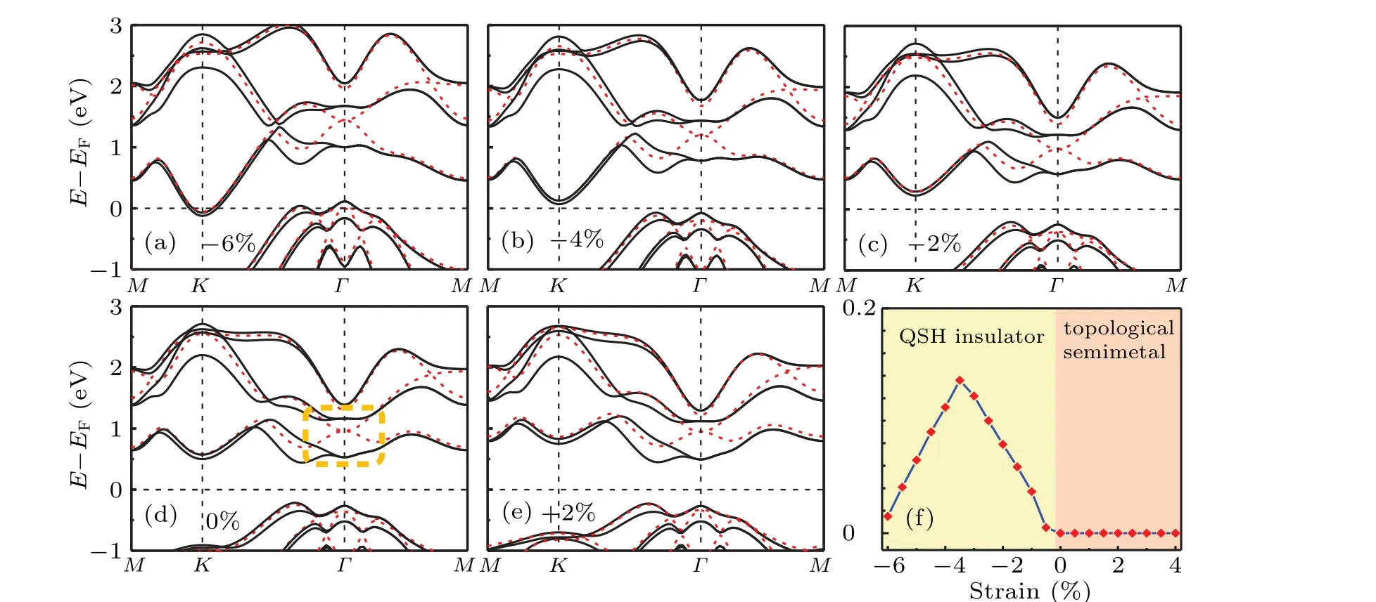
Fig.5. (a)-(e)The band structures of the γ-TeSe2 monolayer under strain of different strengths. The red dotted and black solid curves give the bands without and with SOC,respectively. (f)The global band gap as a function of the strain for the γ-TeSe2 monolayer. Obvious topological phase transition occurs with compressive strain applied.
As shown in Fig.5,with the increase of the compressive strain(from Fig.5(d)to Fig.5(a)),the relative position of the characteristic doubly degenerate bands at theΓpoint moves to high energy region (from 1.0 eV in Fig. 5(d) to 1.4 eV in Fig.5(a)). Clearly,the dispersion of the local bands along theK-Γpath in this energy region decreases in the process,which is beneficial to the opening of the global band gap.In the same process,the minimum band gap along theK-Γpath,however,decreases,hampering the opening of the global band gap. The competition of these two respects gives rise to the global band gap increasing first and then decreasing as the increase of the compressive strain,as displayed in Fig.5(f). The global band gap of the system reaches the maximum of 0.14 eV with the strain ofε=?3.5%. In the absence of strain or under tensile strain,theγ-TeSe2monolayer owns a semimetallic state with a higher electronic conduction performance than the semiconductors because of its‘quasi’metallic band structures.
The movement of the doubly degenerate bands at theΓpoint (marked by the yellow rectangle in Fig. 5(d)) under the compressive strain can be comprehended by the orbitalresolved densities of states (DOSs) of the Se1 and Te atoms shown in Fig. 6. Note that due to theC3vsymmetry owned by theγ-TeSe2monolayer, the DOSs of pxand pyorbitals of the Se1 (also Te) atoms are completely overlapped in Fig. 6.The unoccupied states of the Te atom are much more than that of the Se atoms,hinting the charge transfer from the Te to Se atoms, consistent with the above analysis. These multivalent states,similar to the cases of the tellurene and MoS2systems,ensure the structural stability of theγ-TeSe2monolayer. In Fig. 6(a), the Se1 p orbitals are mainly distributed between?2 eV and?0.5 eV together with a few distributions between?6 eV and?2 eV or between 0.5 eV and 2.8 eV.The Te p orbitals are mainly distributed between?6 eV and?2 eV or between 0.5 eV and 2.8 eV.Unlike the Se1 atom,the Te p orbitals are not distributed between?2 eV and?0.5 eV,corresponding to the nonbonding state between Te and Se as discussed in Fig.4. With the increase of the compressive strain,the Te-Se bond length decreases (Table 2). Thus, the Te-Se bonds become strong,leading to the bonding and antibonding states moving to the lower and higher energy regions, respectively.This trend can be seen obviously from Figs. 6(a)-6(d). For example,the antibonding states of the Te and Se atoms move from the energy region of 0.5-1.5 eV in Fig.6(a)to the energy region of 0.8-3.0 eV in Fig. 6(c). This behavior rationalizes well the movement to a high energy of the doubly degenerate bands at theΓpoint marked in Fig.5(d)with the increase of the compressive strain.
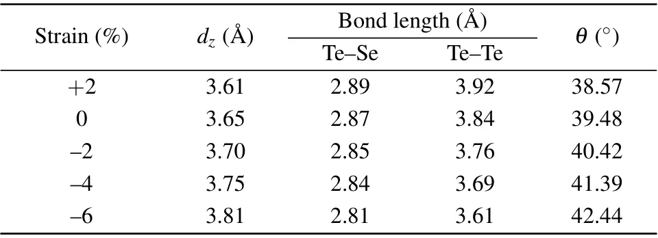
Table 2. The structural parameters of the γ-TeSe2 monolayer under strain, including the layer thickness dz in the z direction, bond lengths of Te-Se and Te-Te,and angle θ between the Te-Se bonding direction and the horizontal direction(shown in Fig.1).
We now understand the variation of the local band gap,marked by the red circle in Fig. 7(a), forγ-TeSe2under the compressive strain. As displayed in Fig. 7, this local band gap is opened due to the direct interactions between the px,py(also few pz) orbitals of Se and the px, pyorbitals of Te.With the increase of the compressive strain, the band gap decreases. The reason can be due to the decrease of the interactions between the px,pyorbitals of Se and the px,pyorbitals of Te. With the increase of the compressive strain, the layer thickness(dz)increases(Table 2), causing the increase of the distance between Se and Te along thezdirection. Thus,the direct interactions between the px,pyorbitals of Se and the px,pyorbitals of Te decrease.This trend is not beneficial for opening the global band gap after the SOC is taken into consideration.The combination of the variation of the band gap(marked by the red circle in Fig.7(a))and the movement to a high energy of the doubly degenerate bands(marked by the red triangle in Fig.7(a))under strain produces the global band gap increasing first and then decreasing with the increase of the compressive strain,as shown in Fig.5(f).The movement to a high energy of the doubly degenerate bands around 1.0 eV in Fig. 7(a) with the increase of the strain reflects the dispersion decrease of the local bands along theK-Γpath in the process. Thus, the opening of the global band gap in theγ-TeSe2monolayer can be understood by the competition between the decrease of the local band dispersion and the weakening of the interactions between the Se px,pyorbitals and Te px,pyorbitals during the process.
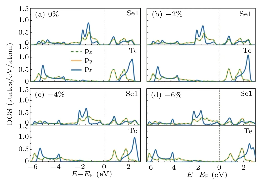
Fig. 6. (a)-(d) The orbital-resolved densities of states of Se1 and Te atom in the γ-TeSe2 monolayer without and with ?2%,?4%,and ?6%strain,respectively. The SOC is not considered. The green,yellow,and blue colors represent the contributions from the px, py, and pz orbitals of the corresponding atom,respectively.

Fig.7.(a)-(d)The energy band projection of the Se1 and Te atoms in the γ-TeSe2 monolayer without and with ?2%,?4%,and ?6%strain,respectively.The SOC is not considered. The green,yellow,and blue colors represent the contributions from the px,py,and pz orbitals of the corresponding atom,respectively.
3.3. Topological properties of γ-TeSe2
Since the concerned global band gap is located around 1.2 eV above theEF, it should be shifted down to theEFfor the transport measurement or applications, which can be achieved by adding two additional electrons per unit cell to theγ-TeSe2monolayer. Figure 8(a) shows the energy bands of the?4% strainedγ-TeSe2monolayer with two electrons added per unit cell.The electron doping concentration is about 1.5×1015cm?2,which can be experimentally realized via the current gating technologies.[51]In Fig. 8(a), theEFnow lies exactly within the band gap. The topological behavior of the band gap can be explored based on Fig.8(a). Before calculating the topological invariants of theγ-TeSe2monolayer, the energy bands obtained from the DFT are fit with the Wannier function interpolation method. The results are shown in Fig. 8(b), indicating high consistency between the two methods. TheZ2topological invariant is then obtained by calculating the evolution of the Wannier function center,[52]and the result is given in Fig.8(c). The number of intersections between any horizontal reference line and the Wannier function center evolution line in half of the Brillouin zone is odd. Thus, the energy band gap concerned hasZ2=1 and a QSH insulator is obtained for theγ-TeSe2monolayer. The edge states are also investigated for the system. Figure 8(d) displays the energy bands of a semi-infiniteγ-TeSe2monolayer.In the characteristic energy gap,besides a series of trivial edge states caused by the dangling bonds of the open boundary,a pair of edge states(marked by two small black arrows)appears, which connects the bottom of the conduction band and the top of the valence band. They are,thus,protected by the bulk topology. The appearance of the edge states as well as the obtainedZ2=1 in the monolayer shows that the global energy gap obtained in theγ-TeSe2monolayer is topologically nontrivial. The system remains a topologically nontrivial semimetal if tensile strain is applied as indicated in Fig.5(f).
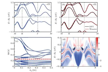
Fig.8. (a)Energy bands of the ?4%strained γ-TeSe2 monolayer after doping two electrons into the unit cell. The EF is now within the global topologically nontrivial band gap. (b)Comparison of the energy bands obtained by using the Wannier function interpolation method and the DFT.(c)The Wannier charge center evolution diagram of the material. (d)The energy bands of a semi-infinite monolayer γ-TeSe2 with ?4%strain. The topologically nontrivial edge states of the material are marked by arrows.
4. Conclusions
Based on the density functional theory and Wannier function method, we studied the electronic states and topological properties of the TeSe2monolayer. Numerical results show that the stableα-TeSe2,β-TeSe2, andγ-TeSe2are semiconductor materials with indirect gaps. Theα-TeSe2is the most stable and a double degeneracy phenomenon is found in the bands ofα-TeSe2andβ-TeSe2. When the compressive strain increases from 0% to 6%, the global topologically nontrivial band gap ofγ-TeSe2is opened and increases first and then decreases. The trend is comprehended based on a competition mechanism. When the compressive strain of 3.5%is applied,theγ-TeSe2monolayer has the maximum global topologically nontrivial band gap of 0.14 eV. The topologically nontrivial feature of the material is characterized by the calculatedZ2topological invariant and the edge state. Theγ-TeSe2remains a topological semimetal with tensile strain up to 4%.Our work shows that group-VI binary 2D compounds can be new type topological materials and have potential applications in the future electronics and spintronics.
Acknowledgement
The calculations were performed at the High Performance Computational Center (HPCC) of the Department of Physics at Fudan University.
猜你喜歡
小資CHIC!ELEGANCE(2021年29期)2021-08-14
法律史評論(2020年1期)2020-09-11
新疆藝術(2018年5期)2018-11-28
中華家教(2018年9期)2018-10-19
作文大王·低年級(2016年10期)2016-10-13
小天使·五年級語數英綜合(2016年8期)2016-08-23
海南熱帶海洋學院學報(2014年1期)2014-08-08
小小說月刊·下半月(2014年6期)2014-05-14
Defence Technology(2011年3期)2011-07-25
- Chinese Physics B的其它文章
- Numerical investigation on threading dislocation bending with InAs/GaAs quantum dots*
- Connes distance of 2D harmonic oscillators in quantum phase space*
- Effect of external electric field on the terahertz transmission characteristics of electrolyte solutions*
- Classical-field description of Bose-Einstein condensation of parallel light in a nonlinear optical cavity*
- Dense coding capacity in correlated noisy channels with weak measurement*
- Probability density and oscillating period of magnetopolaron in parabolic quantum dot in the presence of Rashba effect and temperature*