
Microstructure Functional Devices—Effectively Manipulate Terahertz Waves
2014-03-24 05:40FeiFanJiNingLiSaiChenandShengJiangChang
Fei Fan, Ji-Ning Li, Sai Chen, and Sheng-Jiang Chang
Microstructure Functional Devices—Effectively Manipulate Terahertz Waves
Fei Fan, Ji-Ning Li, Sai Chen, and Sheng-Jiang Chang
——Terahertz (THz) technology promises important applications including imaging, spectroscopy, and communications. However, one of limitations at present for advancing THz applications is the lack of efficient devices to manipulate THz waves. Here, our recent important progresses in THz functional devices based on artificial microstructures, such as photonic crystal, metamaterial, and plasmonic structures, have been reviewed in this paper, involving the THz modulator, isolator, and sensor. These THz microstructure functional devices exhibit great promising potential in THz application systems.
Index Terms——Artificial microstructure, metamaterial, photonic crystals, plasmonics, terahertz.
1. Introduction
The recent progress in terahertz (THz) sources and detectors is turning the “terahertz gap” into one of the most rapidly growing technological fields. High-performance active devices to control and manipulate THz waves are highly desired to develop THz communication and imaging systems[1],[2], such as modulator[3], tunable filter[4], sensor[5], and isolator[6]. In recent years, the artificial electromagnetic materials, such as photonic crystal (PC)[7], photonic crystal fiber[8], metamaterial[9], and plasmonic devices[10], have been extensively investigated in the THz regime, and these devices have been proved both theoretically and experimentally an effective way to transmit as well as control THz waves.
In this paper, we reviewed our proceedings in THzmicrostructure functional devices mainly in recent years, involving THz modulators, filters, isolators, and sensors. For THz modulators, we demonstrated two important device structures for THz wave modulation mechanisms: one is the phase-transition PC and the other is the metal-semiconductor plasmonic waveguide. Then we showed two THz sensors, one is a novel THz microfluidic sensing based on the guided resonance effect in THz PC pillar array; the other is a THz stress sensing based on the flexible THz metamaterials. At last, we demonstrated four different THz microstructure magneto-optical (MO) devices based THz PCs and plasmonic structure with different THz magneto-optical materials, which have important functions of nonreciprocal transmission as a THz isolator and magnetically controlled THz wave modulation. These THz microstructure functional devices exhibit great promising potential in THz application systems.
2. THz Modulators
As a key component for THz applications, many kinds of THz modulators based on PC[11], metamaterial[12], plasmonics[13], and graphene[14]have been demonstrated. However, the transmission bandwidth, modulation depth, and rate of these devices are limited by dielectric constant, loss, and response time of the materials used in these devices. Therefore, to achieve high-speed modulation or filtering for broadband THz radiation, it is necessary to find high-speed, low-loss THz functional materials, and design novel structures. Here, we show two different mechanisms for THz wave modulation: one is phase-transition PC, and the other is metal-semiconductor plasmonic waveguide.
2.1 Phase-Transition Photonic Crystals
In recent researches, vanadium dioxide (VO2) shows great potential in THz wave modulation. It undergoes an insulator-metal transition (IMT) at critical temperatureTc=340 K[15], and its lattice structure changes from insulating phase to metallic phase with its conductivity changing 3-5 orders of magnitude induced rapidly by thermal[16], electrical[17], or optical[18]means. For example, more than 65% intensity modulation for the THz waves was achieved by Wenet al.[19]by using a tunable metamaterial with VO2cut-wire resonators. All-optical ultrafast control of THz radiation through a nanopatterned VO2film was demonstrated by Choiet al.[20].
PCs have proved to be an effective way to transmit and control THz waves. PCs for high quality switching and filtering have been widely studied due to their potential applications[4],[7]. We proposed a novel concept of phase-transition PC (PTPC)[21],[22]for the controllable THz device. The interconversion between the dielectric and metallic state of this PTPC with quite different photonic band gaps as shown in Fig. 2 can be realized in a single device structure. VO2film was coated on the whole Si column and the substrate to realize the PTPC. The scanning electron microscope (SEM) images of the fabricated PCs are shown in Fig. 1. When VO2film is on the insulating phase, this PC shows the properties of a dielectric PC. After the IMT of VO2film, this PC turns to the characteristics of metallic PC. In this IMT process, the transmission property in the periodic plane of the PTPC is dramatically changed, and thus THz waves are modulated by this PTPC.

Fig. 1. SEM images of the fabricated PC: (a) Si PCs without VO2coating and (b) phase-transition PCs with VO2coating.

Fig. 2. Band structures of PTPC: (a) dielectric state and (b) metallic sate[21].

Fig. 3. Transmission spectra in the periodic plane of the PTPC with the different conductive states: (a) from dielectric state to loss state and (b) from loss state to metallic state[21].
As shown in Fig. 3, the whole transition can be divided into two processes. The first process refers to the transition from a dielectric state PC to the loss, so it realizes the intensity modulation for THz waves in the frequency ranges of 0.68 THz-0.8 THz and 1.02 THz-1.25 THz. The second process refers to a transition from the loss state to a metallic state PC, and the intensity modulation for THz waves in the frequency range of 0.8 THz-1.45 THz is also realized. This novel modulation mechanism is derived from the shift of the photonic bandgaps accompanying with the IMT of VO2.
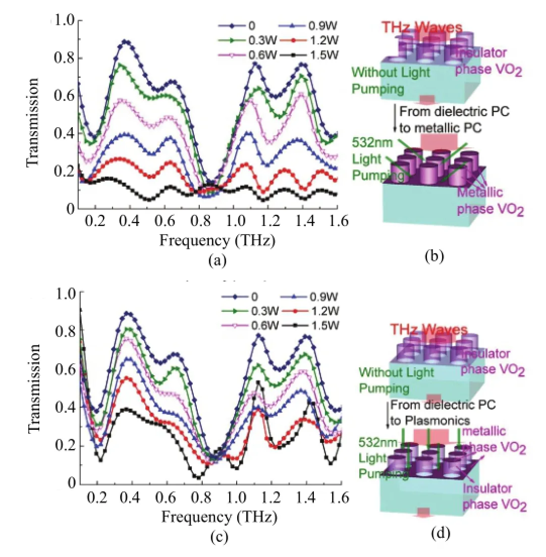
Fig. 4. Transmission spectra of the PTPC with different pump power: (a) under the double 45°tilted pumping, (b) model sketch of the state conversion from a dielectric PC to a metallic PC, (c) under the normal pumping, and (d) model sketch of the state conversion from a dielectric PC to a disk+hole array plasmonics with partial IMT in geometry[22].
We introduced another THz modulator based on the PTPC induced by optical pumping. With different pump powers and angles, this device demonstrates different modulation properties. First, we measured the transmission spectra of the PTPC under the double 45°tilted pumping as shown in Fig. 4 (a). With the pump power increasing, the whole VO2shell gradually changes from insulating to metallic phase as shown in Fig. 4 (b). Accordingly, a broadband intensity modulation for THz waves was achieved with 70% modulation depth at 0.3 THz-0.7 THz and 1.05 THz-1.45 THz bands. Second, we measured the THz transmission spectra of the PTPC with different pump powers under the normal pumping. As shown in Fig. 4 (c), the transmittances outside the resonance in the spectra gradually decline with the pump power increasing, while two new transmission peaks generate at 1.17 THz and 1.44 THz when the pump power is larger than 1.2 W. The above phenomena can be explained by the model shown in Fig. 4(d). Due to the normal pumping, the VO2film on the column sidewall cannot be excited, so it keeps the insulting phase, and only the VO2films on the top and substrate change to the metallic phase, forming a special plasmonic device periodically structured by a metallic disk overhead a metallic hole with the same diameter. The new transmission peaks originate from the extraordinary optical transmission of this structure. This PTPC modulation scheme will be of great significance for THz applications.
More details for this research can be found in our recent publications in [21] and [22].
2.2 Metal-Semiconductor Plasmonic Waveguide
In recent years, considerable efforts have been devoted to manipulate THz waves with approaches including semiconductor[23],[24]or graphene[25]-[27]in two-dimensional electron gas systems and metamaterials with a charge carrier injection/depletion scheme, such as Schottky diodes[3],[28]and high-electron-mobility transistors[29],[30]. However, the performances of the above THz devices are still limited in modulation depth, operating voltages, and modulation rate due to their two-dimensional plane structure which leads these devices lack of strong light-material interactions on the direction of THz wave propagation. When a periodic metal or semiconductor structure along the light propagation direction is engineered, a plasmonic band structure can be exhibited. Such a structure supports strongly confined surface waves with a dispersion relation of surface plasmon polaritons, namely plasmonic crystal waveguide[31],[32].
Therefore, here we introduce a cross-shaped metalsemiconductor plasmonic waveguide (MSPW)[33]in the THz regime, of which the structure is shown in Fig. 5, and focus on its transmission and tuning properties. According to the mode analysis, we find that the different resonance modes of the MSPW show the different changes when the carrier density in the semiconductor is changed. This MSPW realizes an intensity modulation at 0.5 THz and 1.1 THz with nearly 100% modulation depth.
More details for this research can be found in our recent publication in [33].

Fig. 5. Cross-shaped MSPW THz modulator: (a) schematic view, (b) structure of unite cell, and (c) transmission spectra of MSPW with the different doped InSb of 1 S/m-2×105S/m[33].

Fig. 6. Electrically controlled double-structured Scholttky gate arrays: (a) schematic diagram of the device chip and THz waves propagation through the device chip arranged in the TPPWG and (b) SEM image of the device chip.

Fig. 7. Power transmission spectra of the device measured by THz-TDS experiments (a) under positive biases and (b) negative biases.

Fig. 8. Plasmonic bands of the deivce: (a) 0 V, (b) -15 V, (c) 15 V, and (d) models of plasmonic crystals and its energy levels.
Based on the above research about MSPW, we presented another electrically controlled THz plasmonic crystal waveguide based on double-structured Schottky gate arrays as shown in Fig. 6. Schottky barrier under the metal gratings can be controlled by using different positive and negative biases, which leads to the changes of THz SPPs (surface plasmon polaritons) overlapped with the Schottky barrier. THz modulations with a 15 dB modulation depth have been realized in the frequency of 2.2 THz-3.2 THz as shown in Fig. 7. Interestingly, it exhibits two different modulation behaviors: the THz SPP occurs to a discreteresonance frequency jump when applying positive bias as shown in Fig. 7 (a), while it turns to a continuous shift when applying negative bias as shown in Fig. 7 (b). The simulations and theoretical model demonstrate and well explain the shifting and coupling behaviors of the doubled plasmonic band series with the changes of the Schottky barriers in this device. We have proved this phenomenon corresponds to special doubled plasmonic band series due to the double-structured Schottky barrier gratings as shown in Fig. 8. Therefore, we presented a novel mechanism in THz plasmonics that is a plasmonic analogue of the band transition behaviors in the diatomic lattice as shown in Fig. 8 (d). This controllable THz modulation chip can be feasibly integrated with other THz solid-state electronics and promote the practical application of THz communication.
3. THz Sensors
THz sensing of chemical and biomedical compositions, especially microfluidic sensing, have revealed attractive potential by using the recently developed terahertz time-domain spectroscopy (THz-TDS), and considerable researches for highly sensitive sensors have been demonstrated in this field[34]-[38]. For example, plane metamaterial[36]and metal hole array[37]have been used to detect DNA and other liquid or gas materials on the surface of these on-chip devices. A crucial limitation based on these planar geometries is not compatible with dynamical online process or quantitative monitoring. Here, we show a THz microfluidic sensing based on a novel guided resonance effect in a THz PC pillar array and a THz strain sensing based on the flexible THz metamaterials.
3.1 Microfluidic Sensing Based on the Guided Resonance in THz PC Pillar Rrray
The guided resonance (GR), which is a discrete leaky mode that lies above the light line in the photonic band structure, can leak out of the PC plane and couple to the free-space waves to produce sharp resonant features. This effect was mainly investigated in the PC hole slab in the previous reports[39]-[42].
Here, a guided resonance (GR) effect in THz PC pillar array quite different from the GR effect in PC hole slab has been discovered in the experiment as shown in Fig. 9 (a). We found a strong correlation between this GR and the photonic band gaps of the PC, and demonstrated these resonances in the THz PC pillar are the analogue of dipole transitions, which originate from the coupling between the free-space wave and the periodic plane of PC pillar at the photonic band gap center. And we built the symmetry line shape model for this GR in theory, and demonstrated its relation and transition with the asymmetry Fano line shape. The influences of the incident angles (shown in Fig. 9 (b)) and the refractive index of surrounding material have been demonstrated, which experimentally confirms the mutual transition between the symmetry and asymmetry line shape in this PC system. This research deepens understanding on the physical relation and mutual transition between the Lorentz symmetry resonance and Fano asymmetry resonance in artificial electromagnetic microstructure in theory, and we introduced the microfluidic sensing based on these PC chips. This sensing strategy has no coupling problem and the 3D structure of PC pillar is compatible with liquid flow and monitoring different liquid amount, and therefore can be more easily implemented in real-time quantitative microfluidic sensing[43].

Fig. 9. Guided resonance effect in PC arrays: (a) experimental (dots) and theoretical (lines) transmission spectra of three PC samples and (b) experimental transmission spectra of PC1 with different incident angles.
For qualitative monitoring experiment, three types of volatile liquids, i.e. ethanol, acetone, and petroleum ether, filled with the PC1 were tested. As shown in Fig. 10, the frequency positions and transmittances of each resonance marked in Fig. 10 are different. These differences depend on the refractive index and absorption coefficient of different liquid in the THz region. Therefore, each liquid has a characteristic spectral line, so we can identify the kind of liquid to achieve qualitative monitoring.

Fig. 10. Experimental amplitude transmission spectra of ethanol, acetone, and petroleum ether fully filled with the PC1 chip[43].
For quantitative sensing experiment, we measure the THz transmission spectra series after dropping the liquid for the different delay timeTd, and the results for the ethanol on the PC1 chip are shown in Fig. 11 (a). The experimental results indicate that the amount decline of the microfluidic is reflected in the spectral changes at the different delay time. To establish a relation between theexperimental data and the practical liquid amount, we simulated the transmission spectra of the model shown in Fig. 11 (b). EachTdshown in Fig. 11 (a) can find a corresponding layer thickness shown in Fig. 11 (b), so the exact amount of the microfluidic at each moment can be determined. It is notable that a good linear relation between the amount of ethanol and the delay time, and the slope indicates the decline rate of the ethanol microfluidic on the PC chips due to the flow and volatilization. Therefore, these PC sensor chips and terahertz sensing method have great promising potential in the non-contact dynamical monitoring and real-time quantitative sensing.
More details for this research can be found in our recent publication in [43].

Fig. 11. THz real-time quantitative microfluidic sensing based on PC arrays: (a) experimental amplitude transmission spectra series after dropping the ethanol on the PC chip for the different delay times, and (b) simulated amplitude transmission spectra series of the ethanol layer with different thickness[43].
3.2 Strain Sensing Based on the Flexible THz Metameaterials
Metamaterials refer to artificial composites made of dense arrays of sub-wavelength resonators. They allow manipulation of electromagnetic waves in unique ways[9]. Based on the controllable electromagnetic properties, metamaterials promise unprecedented opportunities to explore a variety of applications, including superlenses, cloaks, perfect absorbers, and sensors. Most metamaterials provide functionality only within a narrow spectral range; however, in many cases it is desirable to adapt a metamaterial to its environment by tuning its frequency.
The advancement of polymer technologies and lithographic techniques makes it possible to fabricate terahertz metamaterials on thin flexible substrates[44]-[46]. The resonance frequency could be shifted and fully recovered as a function of the applied strain along the polarization axis. Here, we presented the fabrication and characterization of flexible THz metamaterials for mechanical tuning and strain sensing. Applying a stretching force to the substrate changes the inter-cell capacitance and hence the resonance frequency of the resonators as shown in Fig. 12. Greater than 8% of the tuning range is achieved with a good repeatability over several stretching-relaxing cycles. Therefore, our metamaterials exhibit good stretchability and recoverability. Moreover, we experimentally demonstrated a four-fold symmetric flexible metamaterial. Two independent resonances can be observed when the structure is probed with linearly polarized terahertz waves in two orthogonal axes as shown in Fig. 13. Applying a stretching force causes an observable frequency shift in the corresponding resonance, with minimal effect on the other. This study suggests a possible application of flexible metamaterials for strain sensing.

Fig. 12. Strain sensing based on the flexible THz metamaterials: (a) fabricated THz I type flexible metamaterials and (b) experimental and simulation spectra when structures are stretched from 0 to 10Δl0with a step size of Δl0[47].

Fig. 13. experimental and simulation spectra of four-fold symmetric flexible metamaterial when structures are stretched from 0 to 10Δl0with a step size of Δl0[48].
More details for this research can be found in our recent publications in [47] and [48].
4. THz Isolators and Other Magneto-Optical Devices
THz magneto-optical (MO) devices are indispensable in isolation[6], polarization controlling[49], modulation, and enhancement[50], which can be feasibly controlled by an external magnetic field (EMF). The limitation for developing THz MO device is mainly lack of materials with a strong MO activity and low loss in the THz regime. In spite of this, some recent progresses in this field have been reported. For examples, the giant Faraday rotations were observed in some high electron mobility semiconductors, such as InSb[51], HgTe[52], and graphene[53]. A magnetically induced THz transparency (a sudden appearance and disappearance for THz transmission) in then-doped InSb was demonstrated, owing to the interference between left and right circularly polarized magnetoplasmon (MP) eigenmodes[54]. The tunable THz MPs and MO splitting were observed in the monolayer graphene[55]and patterned graphene disk arrays[56]. However, the improvement of THz MO devices is still challenging.
In the THz regime, due to lack of feasible low-loss, broadband one-way transmission devices, such as isolator and circulator, the THz echo of the reflection and scattering for system components bring some noise severely limiting the performance of these THz systems. In recent years, a number of nonreciprocal photonic devices have been investigated in the microwave and near-infrared regime. In this section, we introduced a silicon-ferrite PC cavity for THz circulator and the metal/magneto-optical plasmonic waveguide and plasmonic lens for THz isolator in turn. At last, we introduced a novel MO nanomaterial for THz waves, and its application in THz controllable MO device.
4.1 Silicon-Ferrite PC Cavity
Circulator is a kind of nonreciprocal devices as shown in Fig. 14 (a)[57],[58]. A small absorption loss and the existences of the ferromagnetic resonance indicate that the ferrite is a kind of promising materials for THz waves[59],[60]. Here, we introduce a silicon-ferrite PCs circulator in the sub-THz region as shown in Fig. 14 (a)[61]. Through the structure optimization and analysis of defect mode coupling, we designed a magnetically tunable circulator, of which central operating frequency can be tuned from 180 GHz to 205 GHz and the maximum isolation is 65.2 dB as shown in Fig. 14 (d). The defected rotating dipole mode and the field patterns at operating frequency are shown in Figs. 14 (b) and (c). We find that, on the one hand, the PC cavity affects the mode confinement and spatial overlap of the magnetic material domain and defect modes; on the other hand, the gyrotropy and ferromagnetic loss of the ferrite also greatly affect the transmission and isolation property of this device as a function of MF and THz frequency. This circulator can realize the controllable splitting, filtering, and isolating for THz applications.
More details for this research can be found in our recent publication in [61].
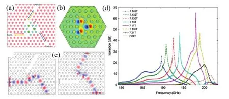
Fig. 14. Silicon-ferrite PC for THz circulator: (a) schematic diagram, (b) electric field pattern of defected rotating dipole mode, (c) electric field patterns of the circulator, and (d) isolation spectra under the different EMF[61].
4.2 Metal/Magneto-Optical Plasmonic Waveguide
In addition to the ferrite, doped semiconductor can be also used as magneto-optical material in the THz regime. Because the cyclotron frequency of high electron mobility semiconductor[51]-[53], such as InSb, is located in the THz regime, which shows gyrotropy properties under a relatively small EMF, the one-way transmission can be realized[62]. Moreover, many reports show that not only the gyrotropy of the material but also the structures of the device determine the nonreciprocity of the one-way waveguide, and the optimized designs could greatly enhance the one-way transmission of the device. Therefore, we proposed a tunable THz isolator based on a metal/magneto-optical plasmonic waveguide (MMOPW)[63]as shown in Fig. 15 (a). Due to the introduction of periodic structure, the MMOPW shows a unique photonic band-gap characteristic that greatly enhances the one-way transmission, and obtains a lower insertion loss and higher isolation.

Fig. 15. THz isolator based on metal/magneto-optical plasmonic waveguide: (a) schematic structure of the proposed MMOPW, (b) band structure of the MMOPW whenT=195 K,B=1 T, (c) isolation spectra of the SMPW under the different EMF atT=195 K, and (d) electric field distributions of the SMPW whenT=195 K andB=1 T of 1.2 THz forward wave and backward wave[63].
Based on the dispersion and gyrotropy property of the InSb, the non-symmetrical photonic band-gap and one-way transmission property of the MMOPW are investigated in the THz regime. Due to the nonreciprocity of the InSb under the MF and the non-symmetry boundary conditions, the time reversal symmetry of the waveguide is broken, so the dispersion curves in the positive and negative propagation direction are different[64],[65]. Fig. 15 (b) shows the dispersion relation of the MMOPW atT=195 K withB=1 T. The dispersion curves show a significant photonic band structure due to the periodic structure of the SMPW.For the forward wave, a passband with high transmittances locates in 1.16 THz-1.28 THz, and the maximum transmittance is 95%. For the backward wave, no backward waves can propagate through the MMOPW in this frequency bands. As can be seen from the isolation spectra in Fig. 15 (c), the device obtains its 30 dB isolation spectral width of larger than 80 GHz, the maximum isolation of higher than 90 dB at 1.18 THz, and the corresponding insertion loss of less than 5%. The further discussions show that the operating frequency band of this MMOPW isolator can be controlled by magnetic and thermal means.
More details for this research can be found in our recent publications in [63].
4.3 Metal/Magneto-Optic Plasmonic Lens
Plasmonic lens (PL) can focus light beyond diffraction limit by means of SPPs, which has attracted much attention recently due to its unique feature of extraordinary enhanced transmission[66],[67]. The different phase retardations can be achieved by structuring the PLs to manipulate the spatial distribution of the output beam. So we introduce another THz isolator composed by a slit array with a periodic arrangement of the metal and InSb grating in turn as shown in Fig. 16 (a) called metal/magneto-optic plasmonic lens (MMOPL). Compared with the previous single waveguide isolators, our MMOPL structure is an area array device[68]. Since our structure is larger than the area of THz beam, we do not need compressing THz beam to subwavelength scale to couple it into a single waveguide structure by using any couplers, so the MMOPL has a smaller insertion loss.

Fig. 16. THz isolator based on metal/magneto-optical plasmonic waveguide: (a) schematic structure of the proposed MMOPL, (b) forward and (c) backward power flow distributions through the MMOPL at 1.25 THz, and (d) dispersion relations of MMOPL at 185 K and 0.5 T, and (e) isolation spectra of the MMOPL under the different MF at 185 K[68].
The asymmetrical dispersion relations of the proposed MMOPL are investigated in the THz regime as shown in Fig. 16 (d). When there is no EMF applied, the dispersion curve is symmetric for the forward and backward propagation. When an EMF is applied as shown in Fig. 16 (d), due to the gyrotropy of the InSb under the EMF and the non-symmetry structure, the SPPs split as two different MSPPs. Thus the dispersion curve becomes non-symmetric, the branch of the forward propagation moves to a higher frequency, and the backward moves to a lower frequency. For the backward wave, its bandgap is located at 1.45 THz-1.55 THz (yellow region in Fig. 16 (d)), while the forward wave can still transmit at this frequency range. Therefore, this is an isolation region which permits the forward wave but forbids the backward wave.
The numerical results show that the proposed isolator has an isolation bandwidth of larger than 0.4 THz and the maximum isolation of higher than 110 dB at the temperature of 185 K as shown in Fig. 16 (e). The operating frequency of this device also can be broadly tuned by changing the external magnetic field or temperature. The further discussions show that a transmission enhancement through this MMOPL is about 30 times larger than that of the ordinary PLs. This low-loss, high isolation, and broadband tunable nonreciprocal THz transmission mechanism has a great potential application in promoting the performances of the THz application systems.
More details for this research can be found in our recent publications in [68].
4.4 Ferrofluid-Filled Photonic Crystal
Ferrofluid is a colloidal suspension composed of magnetic nanoparticles in a carrier liquid, of which optical and MO properties have been extensively investigated in the optical frequency range[69],[70]. The ferrofluid has advantages due to its liquid form and low EMF requirement, especially in liquid-filled photonic devices[71],[72]. However, its optical and MO property in the THz regime have still been rarely reported yet, and until recently, Shalabyet. al. has demonstrated the ferrofluid has a very low absorption loss and a certain MO activity under a low EMF in the THz regime[73], but its Faraday rotation is not adequate for a THz Faraday isolator. The combination between artificial electromagnetic materials and MO materials may enhance the MO effect in the device. For examples, in the optical regime, both an enhanced Voigt MO effect[74]and a giant enhancement of Faraday rotation[75]in a garnet-metal grating were demonstrated, respectively. Therefore, filling the ferrofluid into an artificial electromagnetic materials structure may enhance the MO response in the THz regime. Here, We investigated THz MO properties of a ferrofluid and a ferrofluid-filled photonic crystal (FFPC)[76]by using the THz-TDS.
The ferrofluid used in this work is Fe3O4nanoparticles dispersed in a light mineral oil carrier. As shown in Fig. 17, when the ferrofluid is not magnetized, the particles are randomly distributed and the fluid can be regarded as an isotropic material. A weak EMF can trigger the particles toform magnetic chain clusters along the EMF direction which exhibits a MO property, and the number of the cluster increases with the EMF increasing until saturated magnetization. The experiment results show that the refractive index and absorption coefficient of ferrofluid for THz waves increase with the nanoparticle concentration increasing in the ferrofluid. Moreover, two different THz MO effects have been found with different EMF, of which mechanisms have been theoretically explained well by microscopic structure induced refractive index change in the magnetization process and the transverse magnetooptical effect after the saturation magnetization as shown in Fig. 18. This work suggests that ferrofluid is a promising MO material in the THz regime.

Fig. 17. Microscope images of ferrofluid: (a) without and (b) with an EMF.

Fig. 18. Optical and magneto-optical property of ferrofluid: (a) Refractive index and (b) the absorption coefficient of the ferrofluid under the different EMF in the THz regime[76].
We applied the EMF as the Voigt configuration as shown in Fig. 19, and the THz transmission spectra of the FFPC are shown in Fig. 20 (a). As the EMF increases, the original resonance dip gradually splits into two resonances. Their resonance frequencies gradually move to lower and higher frequency compared to the original resonance, respectively, and their resonance intensities gradually increase with the EMF increasing. In this process, the transmittance at 1.04 THz gradually rises up from 1.1% at 0 mT to 40% at 150 mT, which experiences a transition from a resonance dip to a transmission peak. Therefore, this FFPC realizes a magnetically induced THz wave transparency at the central frequency of 1.04 THz with 150 GHz bandwidth. This periodically MO-dielectric hybrid model leads the MP mode splitting, and the finite element method simulation confirmed the existence of the CW and CCW rotating MP modes as shown in Fig. 20 (b). This THz microstructure MO device and its tunabilty scheme will have great potential applications in THz filtering, modulation and sensing.
More details for this research can be found in our recent publication in [76].

Fig. 19. Schematic diagram of FFPC[76].

Fig. 20. Magnetically induced THz wave transparency and MP mode splitting effect in FFPC: (a) experiment transmission spectra of the FFPC under the different EMF and (b) dependence of the effective refractive indexes of the CCW and CW MP modes at 150 mT[76].
5. Conclusions
In conclusion, our recent important progress in THz functional devices based on PCs, metamaterials, and plasmonics was reviewed in this paper, involving THz modulators, sensors, and isolators. These recent research progresses imply a great deal of interest regarding the applications of subwavelength functional devices for THz science and technology. As a matter of fact, the interest in THz regime is increasing with the appearance of new sources and detectors that have opened a new range of applications, motivating new studies of subwavelength functional devices in this frequency range.
[1] T. Kleine-Ostmann and T. Nagatsuma, “A review on terahertz communications research,”J. Infrared Milli. Tera. Waves, vol. 32, no. 2, pp. 143-171, 2011.
[2] W. L. Chan, J. Deibel, and D. M. Mittleman, “Imaging with terahertz radiation,”Rep. Prog. Phys., vol. 70, no. 8, pp. 1325, 2007.
[3] H. T. Chen, W. J. Padilla, J. M. O. Zide,et al., “Active terahertz metamaterial devices,”Nature, vol. 444, no. 7119, pp. 597-600, 2006.
[4] H. Zhang, P. Guo, P. Chen,et al., “Liquid-crystal-filled photonic crystal for terahertz switch and filter,”J. Opt. Soc. Am. B, vol. 26, no. 1, pp. 101-106, 2009.
[5] R. Mendis, V. Astley, J. B. Liu,et al., “Terahertz microfluidic sensor based on a parallel-plate waveguideresonant cavity,”Appl. Phys. Lett., vol. 95, no. 17, pp. 171113, 2009.
[6] M. Shalaby, M. Peccianti, Y. Ozturk,et al., “A magnetic non-reciprocal isolator for broadband terahertz operation,”Nature Commun., vol. 4, no. 1558, pp. 1-7 , 2013.
[7] F. Fan, S.-J. Chang, and Y. Hou, “Metallic photonic crystals for terahertz tunable filters,”SCIENCE CHINA Information Sciences, vol. 55, no. 1, pp. 72-78, 2012.
[8] Y. Hou, F. Fan, H. Zhang, X.-H. Wang, and S.-J. Chang,“Terahertz single-polarization single-mode hollow-core fiber based on index-matching coupling,”IEEE Photonic. Tech. Lett., vol. 24, no. 8, pp. 637-639, 2012.
[9] N. I. Zheludev and Y. S. Kivshar, “From metamaterials to metadevices,”Nature Mater., vol. 11, no. 11, pp. 917-924, 2012.
[10] M. Dragoman and D. Dragoman, “Plasmonics: Applications to nanoscale terahertz and optical devices,”Progress in Quant. Electron., vol. 32, no. 1, pp. 1-41, 2008.
[11] L. Fekete, F. Kadlec, P. Ku?el,et al., “Ultrafast opto-terahertz photonic crystal modulator,”Opt. Lett., vol. 32, no. 6, pp. 680-682, 2007.
[12] J. Gu, R. Singh, X. Liu,et al., “Active control of electromagnetically induced transparency analogue in terahertz metamaterials,”Nature Commun., vol. 3, no. 1151, pp. 1-6, 2012.
[13] W. Li, D.-F. Kuang, F. Fan, S.-J. Chang, and L. Lin,“Sub-wavelength B-shaped metallic hole array Terahertz filter with InSb bar as thermally tunable structure,”Appl. Opt., vol. 51, no. 29, pp. 7098-7102, 2012.
[14] L. Ju, B. S. Geng, J. Horng,et al., “Graphene plasmonics for tunable terahertz metamaterials,”Nature Nanotech., vol. 6, no. 10, pp. 630-634, 2011.
[15] P. U. Jepsen, B. Fischer, A. Thoman, H. Helm, J. Y. Suh, R. Lopez, and R. F. Haglund, “Metal-insulator phase transition in a VO2thin film observed with terahertz spectroscopy,”Phys. Rev.B, vol. 74, no. 205103, pp. 1-9, 2006.
[16] P. Mandal, A. Speck, C. Ko, and S. Ramanathan, “Terahertz spectroscopy studies on epitaxial vanadium dioxide thin films across the metal-insulator transition,”Opt. Lett., vol. 36, no. 10, pp. 1927-1929, 2011.
[17] Y. G. Jeong, H. Bernien, J. S. Kyoung, H. R. Park, H. S. Kim, J. W. Choi, B. J. Kim, H. T. Kim, K. J. Ahn, and D. S. Kim,“Electrical control of terahertz nano antennas on VO2thin film,”Opt. Express, vol. 19, no. 22, pp. 21211-21215, 2011.
[18] D. J. Hilton, R. P. Prasankumar, S. Fourmaux, A. Cavalleri, D. Brassard, M. A. Khakani, J. C. Kieffer, A. J. Taylor, and R. D. Averitt, “Enhanced photosusceptibility nearTcfor the light-induced insulator-to-metal phase transition in vanadium dioxide,”Phys. Rev. Lett., vol. 99, no. 226401, pp. 1-4, 2007.
[19] Q.-Y. Wen, H.-W. Zhang, Q.-H. Yang, Y.-S. Xie, K. Chen, and Y.-L. Liu, “Terahertz metamaterials with VO2cut-wires for thermal tunability,”Appl. Phys. Lett., vol. 97, no. 2, pp. 021111-021111-3, 2010.
[20] S. B. Choi, J. S. Kyoung, H. S. Kim, H. R. Park, D. J. Park, B. J. Kim, Y. H. Ahn, F. Rotermund, H. T. Kim, K. J. Ahn, and D. S. Kim, “Nanopattern enabled terahertz all-optical switching on vanadium dioxide thin film,”Appl. Phys. Lett., vol. 98, no. 7, pp. 071105-071105-3, 2011.
[21] F. Fan, Y. Hou, Z.-W. Jiang, X.-H. Wang, and S.-J. Chang,“Terahertz modulator based on insulator-metal transition in photonic crystal waveguide,”Appl. Opt., vol. 51, no. 20, pp. 4589-4596, 2012.
[22] F. Fan, W.-H. Gu, S. Chen, X.-H. Wang, and S.-J. Chang,“State conversion based on terahertz plasmonics with vanadium dioxide coating controlled by optical pumping,”Opt. Lett., vol. 38, no. 9, pp. 1582-1584, 2013.
[23] T. Kleine-Ostmann, P. Dawson, K. Pierz, G. Hein, and M. Koch, “Room-temperature operation of an electrically driven terahertz modulator,”Appl. Phys. Lett., vol. 84, no. 18, pp. 3555-3557, 2004.
[24] T. Kleine-Ostmann, K. Pierz, G. Hein,et al., “Spatially resolved measurements of depletion properties of large gate two dimensional electron gas semiconductor terahertz modulators,”J. Appl. Phys., vol. 105, no. 9, pp. 093707-093707-6, 2009.
[25] B. Sensale-Rodriguez, R. Yan, S. Rafique,et al.,“Extraordinary control of terahertz beam reflectance in graphene electro-absorption modulators,”Nano Lett., vol. 12, no. 9, pp. 4518-4522, 2012.
[26] B. Sensale-Rodriguez, R. Yan, M. M. Kelly,et al.,“Broadband graphene terahertz modulators enabled by intraband transitions,”Nature Commun., vol. 3, no. 780, pp. 1-7, 2012.
[27] S. H. Lee, M. Choi, T.-T. Kim,et al., “Switching terahertz waves with gate-controlled active graphene metamaterials,”Nature Mater., vol. 11, no. 11, pp. 936-941, 2012.
[28] H.-T. Chen, W. J. Padilla, M. J. Cich,et al., “A metamaterial solid-state terahertz phase modulator,”Nature Photon, vol. 3, no. 3, pp. 148-151, 2009.
[29] D. Shrekenhamer, S. Rout, A. C. Strikwerda,et al., “High speed terahertz modulation from metamaterials with embedded high electron mobility transistors,”Opt. Express, vol. 19, no. 10, pp. 9968-9975, 2011.
[30] L. Wang, X. S. Chen, W. D. Hu,et al., “The plasmonic resonant absorption in GaN double-channel high electron mobility transistors,”Appl. Phys. Lett., vol. 99, no. 6, pp. 063502-063502-3, 2011.
[31] C. R. Williams, S. R. Andrews, S. A. Maier, and A. I. Fern,“Highly confined guiding of terahertz surface plasmon polaritons on structured metal surfaces,”Nature Photon, vol. 2, pp. 175-179, Mar. 2008.
[32] G. C. Dyer, G. R. Aizin, S. J. Allen,et al., “Induced transparency by coupling of Tamm and defect states in tunable terahertz plasmonic crystals,”Nature Photon, vol. 7, pp. 925-930, Sep. 2013.
[33] F. Fan, W. Li, W.-H. Gu, X.-H. Wang, and S.-J. Chang,“Cross-shaped metal-semiconductor-metal plasmonic crystal for terahertz modulator,”Photon Nanostruct: Fundam, Appl., vol. 11, no. 1, pp. 48-54, 2013.
[34] H. Yoshida, Y. Ogawa, Y. Kawai,et al., “Terahertz sensing method for protein detection using a thin metallic mesh,”Appl. Phys. Lett., vol. 91, no. 25, pp. 253901, 2007.
[35] C. Debus and P. H. Bolivar, “Frequency selective surfaces for high sensitivity terahertz sensing,”Appl. Phys. Lett., vol. 91, no. 18, pp. 184102, 2007.
[36] Y.-M. Sun, X.-X. Xia, H. Feng,et al., “Modulated terahertz responses of split ring resonators by nanometer thick liquid layers,”Appl. Phys. Lett., vol. 92, no. 22, pp. 221101, 2008.
[37] F. Miyamaru, S. Hayashi, C. Otani,et al., “Terahertz surface-wave resonant sensor with a metal hole array,”Opt. Lett., vol. 31, no. 8, pp. 1118-1120, 2006.
[38] V. Astley, K. S. Reichel, J. Jones,et al., “Terahertz multichannel microfluidic sensor based on parallel-plate waveguide resonant cavities,”Appl. Phys. Lett., vol. 100, no. 23, pp. 231108, 2012.
[39] S. Fan and J. Joannopoulos, “Analysis of guided resonances in photonic crystal slabs,”Phys. Rev. B, vol. 65, pp. 235112 Jun. 2002.
[40] J. S. Li and S. Zouhdi, “Fano resonance filtering characteristic of high-resistivity silicon photonic crystal slab in terahertz region,”IEEE Photon. Tech. Lett., vol. 24, no. 8, pp. 625-627, 2012.
[41] T. Prasad, V. Colvin, and D. Mittleman, “Dependence of guided resonances on the structural parameters of terahertz photonic crystal slabs,”J. Opt. Soc. Am. B, vol. 25, no. 4, pp. 633-644, 2008.
[42] P. Pottier, L. Shi, and Y. A. Peter, “Determination of guided-mode resonances in photonic crystal slabs,”J. Opt. Soc. Am. B, vol. 29, no. 1, pp. 109-117, 2012.
[43] F. Fan, W.-H. Gu, X.-H. Wang, and S.-J. Chang, “Real-time quantitative terahertz microfluidic sensing based on photonic crystal pillar array,”Appl. Phys. Lett., vol. 102, no. 12, pp. 121113, 2013.
[44] M. Walther, A. Ortner, H. Meier, U. Loffelmann, P. J. Smith, and J. G. Korvink, “Terahertz metamaterials fabricated by inkjet printing,”Appl. Phys. Lett., vol. 95, no. 25, pp. 251107, 2009.
[45] Z.-C. Chen, N.-R. Han, Z.-Y. Pan, Y.-D. Gong, T.-C. Chong, and M.-H. Hong, “Tunable resonance enhancement of multi-layer terahertz metamaterials fabricated by parallel laser micro-lens array lithography on flexible substrates,”Opt. Mater. Express, vol. 1, no. 2, pp. 151-157, 2011.
[46] I. E. Khodasevych, C. M. Shah, S. Sriram, M. Bhaskaran, W. Withayachumnankul, B. S. Y. Ung, H. Lin, W. S. T. Rowe, D. Abbott, and A. Mitchell, “Elastomeric silicone substrates for terahertz fishnet metamaterials,”Appl. Phys. Lett., vol. 100, no. 6, pp. 061101-061101-3, 2012.
[47] J.-N. Li, C. M. Shah, W. Withayachumnankul, B. Ung, A. Mitchell, S. Sriram, M. Bhaskaran, S.-J. Chang, and D. Abbott, “Mechanically tunable terahertz metamaterials,”Appl. Phys. Lett., vol. 102, no. 12, pp. 121101, 2013.
[48] J.-N. Li, C. M. Shah, and W. Withayachumnankul, “Flexible terahertz metamaterials for dual-axis strain sensing,”Opt. Lett., vol. 38, no. 12, pp. 2104-2106, 2013.
[49] F. Fan, Z. Guo, J.-J. Bai, X.-H. Wang, and S.-J. Chang,“Magnetic photonic crystals for terahertz tunable filter and multifunctional polarization controller,”J. Opt. Soc. Am. B, vol. 28, no. 4, pp. 697-702, 2011.
[50] G. Monette, N. Nateghi, R. A. Masut, S. Francoeur, and D. M′enard, “Plasmonic enhancement of the magneto-optical response of MnP nanoclusters embedded in GaP epilayers,”Phys. Rev. B, vol. 86, no. 245312, pp. 1-12, 2012.
[51] T. Arikawa, X. F. Wang, A. A. Belyanin, and J. Kono,“Giant tunable Faraday effect in a semiconductor magneto-plasma for broadband terahertz polarization optics,”Opt. Express, vol. 20, no, 17, pp. 19484-19492, 2012.
[52] A. M. Shuvaev, G. V. Astakhov, A. Pimenov, C. Brune, H. Buhmann, and L. W. Molenkamp, “Giant magneto-optical faraday effect in HgTe thin films in the terahertz spectral range,”Phys. Rev. Lett., vol. 106, no. 107404, pp. 1-4, 2011.
[53] R. Shimano, G. Yumoto, J. Y. Yoo, R. Matsunaga, S. Tanabe, H. Hibino, T. Morimoto, and H. Aoki, “Quantum Faraday and Kerr rotations in graphene,”Nat. Commun., 2013, doi: 10.1038/ncomms2866.
[54] X. Wang, A. Belyanin, S. Crooker, D. M. Mittleman, and J. Kono, “Interference-induced terahertz transparency in a semiconductor magneto-plasma,”Nat. Phys., vol. 6, pp. 126-130, Feb. 2010.
[55] I. Crassee, M. Orlita, M. Potemski, A. L. Walter, M. Ostler, Th. Seyller, I. Gaponenko, J. Chen, and A. B. Kuzmenko,“Intrinsic terahertz plasmons and magnetoplasmons in large scale monolayer graphene,”Nano Lett., vol. 12, no. 5, pp. 2470-2474, 2012.
[56] H. Yan, Z.-Q. Li, X.-S Li, W.-J. Zhu, P. Avouris, and F.-N. Xia, “Infrared spectroscopy of tunable dirac terahertz magneto-plasmons in graphene,”Nano Lett., vol. 12, no. 7, pp. 3766-3771, 2012.
[57] Z. Wang and S. Fan, “Magneto-optical defects in two-dimensional photonic crystals,”Appl. Phys. B: Lasers Opt., vol. 81, pp. 369-375, Jul. 2005.
[58] W. Smigaj, J. R. Vivas, B. Gralak, L. Magdenko, B. Dagens, and M. Vanwolleghem, “Magneto-optical circulator designed for operation in a uniform external magnetic field,”Opt. Lett.,vol. 35, no. 4, pp. 568-570, 2010.
[59] Q.-H. Yang, H.-W. Zhang, L.-Y. Li, Q.-Y. Wen, and J. Zha,“An artificially garnet crystal materials using in terahertz waveguide,”Chin. Phys. Lett., vol. 25, no. 11, pp. 3957-3960, 2008.
[60] Q.-Y. Wen, H.-W. Zhang, H.-Q.Yang, S. Li, D.-G. Xu, and J.-Q. Yao, “Fe-doped polycrystalline CeO2as terahertz optical material,”Chin. Phys. Lett., vol. 26, no. 4, pp. 047803, 2009.
[61] F. Fan, S.-J. Chang, C. Niu, Y. Hou, and X.-H. Wang.“Magnetically tunable silicon ferrite photonic crystals for terahertz circulator,”Opt. Commun., vol. 285, no. 18, pp. 3763-3769, 2012.
[62] B. Hu, Q.-J. Wang, and Y. Zhang, “Broadly tunable one-way terahertz plasmonic waveguide based on nonreciprocal surface magneto plasmons,”Opt. Lett., vol. 37, no. 11, pp. 1895-1897, 2012.
[63] F. Fan, S.-J. Chang, W.-H. Gu, X.-H. Wang, and A.-Q. Chen,“Magnetically tunable terahertz isolator based on structured semiconductor magneto plasmonics,”IEEE Photonics Tech. Lett., vol. 24, no. 22, pp. 2080-2083, 2012.
[64] B. Hu, Q.-J. Wang, and Y. Zhang, “Slowing down terahertz waves with tunable group velocities in a broad frequency range by surface magneto plasmons,”Opt. Express, vol. 20, no. 9, pp. 10071, 2012.
[65] B. Hu, Q.-J. Wang, S. W. Kok,et al., “Active focal length control of terahertz slitted plane lenses by magnetoplasmons,”Plasmonics, vol. 7, no. 2, pp. 191-199, 2012.
[66] H.-F. Shi, C.-T. Wang, C.-L. Du, X.-G. Luo, X.-C. Dong, and H.-T. Gao, “Beam manipulating by metallic nano-slits with variant widths,”Opt. Express, vol. 13, no. 18, pp. 6815-6820, 2005.
[67] N. Fang, H. Lee, C. Sun, and X. Zhang,“Sub-diffraction-limited optical imaging with a silver superlens,”Science, vol. 308, no. 5721, pp. 534-537, 2005.
[68] F. Fan, S. Chen, X.-H. Wang, and S.-J. Chang, “Tunable nonreciprocal terahertz transmission and enhancement based on metal/magneto-optic plasmonic lens,”Opt. Express, vol. 21, no. 7, pp. 8614-8621, 2013.
[69] S. Yang, J. Chieh, H.-E. Hornga, C.-Y. Hong, and H.-C. Yang, “Origin and applications of magnetically tunable refractive indexof magnetic fluid films,”Appl. Phys. Lett., vol. 84, no. 25, pp. 5204, 2004.
[70] Z.-Y. Di, X.-F. Chen, S.-L. Pu, X. Hu, and Y.-X. Xia,“Magnetic-field-induced birefringence and particle agglomeration in magnetic fluids,”Appl. Phys. Lett., vol. 89, no. 21, pp. 211106, 2006.
[71] W. Lin, Y. Miao, H. Zhang, B. Liu, Y. Liu, and B. Song,“Fiber-optic in-line magnetic field sensor based on the magnetic fluid and multimode interference effects,”Appl. Phys. Lett., vol. 103, no. 15, pp. 151101, 2013.
[72] Y. Chen, Q. Han, T. Liu, X. Lan, and H. Xiao, “Optical fiber magnetic field sensor based on single-mode-multimodesingle-mode structure and magnetic fluid,”Opt. Lett., vol. 38, no. 20, pp. 3999-4001, 2013.
[73] M. Shalaby, M. Peccianti, Y. Ozturk, M. Clerici, I. Al-Naib, L. Razzari, T. Ozaki, A. Mazhorova, M. Skorobogatiy, and R. Morandotti, “Terahertz Faraday rotation in a magnetic liquid: High magneto-optical figure of merit and broadband operation in a ferrofluid,”Appl. Phys. Lett., vol. 100, no. 24, pp. 241107, 2012.
[74] V. I. Belotelov, I. A. Akimov, M. Pohl, V. A. Kotov, S. Kasture, A. S. Vengurlekar, A. Venu Gopal, D. R. Yakovlev, A. K. Zvezdin, and M. Bayer, “Enhanced magneto-optical effects in magnetoplasmonic crystals,”Nat. Nanotechnol., vol. 6, pp. 370-376, Apr. 2011.
[75] J. Y. Chin, T. Steinle, T. Wehlus, D. Dregely, T. Weiss, V. I. Belotelov, B. Stritzker, and H. Giessen, “Nonreciprocal plasmonics enables giant enhancement of thin-film Faraday rotation,”Nat. Commun., vol. 4, pp. 1599, Mar. 2013.
[76] F. Fan, S. Chen, W. Lin, Y.-P. Miao, S.-J. Chang, B. Liu, X.-H. Wang, and L. Lin, “Magnetically tunable terahertz magnetoplasmons in ferrofluid-filled photonic crystals,”Appl. Phys. Lett., vol. 103, no. 16, pp. 161115, 2013.

Fei Fan was born in Sichuan, China in 1986. He received the B.S. degree from the Tianjin University, Tianjin in 2009 and the Ph.D. degree in optical engineering from Institute of Modern Optics, Nankai University, Tianjin in 2014. He is currently the lecturer with the Institute of Modern Optics, Nankai University. His research interests include terahertz microstructure functional devices and terahertz spectroscopy.

Ji-Ning Li was born in Tianjin, China in 1984. He received the B.S. degree from Nankai University, China in 2007 and the Ph.D. degree in optical engineering from the College of Electronic Information and Optical Engineering, Nankai University in 2013. In 2011 and 2012, he was sponsored to join the
Adelaide T-group as a visiting student. Currently, he holds a postdoctoral fellowship with Nankai University. His research interests include metamaterials and surface plasma in the terahertz frequency range.

Sai Chen was born in Beijing, China in 1990. He received the B.S. degree from the Nankai University, Tianjin in 2012 and entered the Institute of Modern Optics, Nankai University, Tianjin in the same year. He is presently the Ph.D. candidate with the Institute of Modern Optics. His research interests in THz microstructure functional devices and magneto-optical material in the THz regime

Sheng-Jiang Chang received his M. S. degree in laser physics, and Ph. D. degree in optical engineering, from Nankai University in 1993 and in 1996, respectively. From 1998 to 2000, he was invited to City University of Hong Kong and awarded the postdoctoral fellowship with the Department of Electronic Engineering, City University of Hong Kong. Since 2000, he has been with the Institute of Modern Optics, Nankai University, where he is presently a full professor and doctorial supervisor with the College of Electronic Information and Optical Engineering. He holds hundreds of publications and more than 10 patents. His current research involves microstructural terahertz devices, terahertz time-domain spectroscopy technology, digital image processing, and the applications of artificial neural network in pattern recognition.
Manuscript received October 4, 2014; revised November 22, 2014. This work was supported by the National Basic Research Program of China under Grant No. 2014CB339800, the National High Technology Research and Development Program of China under Grant No. 2011AA010205, and the National Natural Science Foundation of China under Grant No. 61171027.
F. Fan, J.-N. Li, and S. Chen are with the Institute of Modern Optics, Nankai University, Key Laboratory of Optical Information Science and Technology, Ministry of Education, Tianjin 300071, China.
S.-J. Chang is with the Institute of Modern Optics, Nankai University, Key Laboratory of Optical Information Science and Technology, Ministry of Education, Tianjin 300071, China (Corresponding author e-mail: sjchang@nankai.edu.cn).
Color versions of one or more of the figures in this paper are available online at http://www.intl-jest.com.
Digital Object Identifier: 10.3969/j.issn.1674-862X.2014.04.009
 Journal of Electronic Science and Technology2014年4期
- Journal of Electronic Science and Technology的其它文章
- Study on Temperature Distribution of Specimens Tested on the Gleeble 3800 at Hot Forming Conditions
- Automatic Vessel Segmentation on Retinal Images
- Family Competition Pheromone Genetic Algorithm for Comparative Genome Assembly
- Quantification of Cranial Asymmetry in Infants by Facial Feature Extraction
- Intrinsic Limits of Electron Mobility inModulation-Doped AlGaN/GaN 2D Electron Gas by Phonon Scattering
- Real-Time Hand Motion Parameter Estimation with Feature Point Detection Using Kinect